University of Sydney
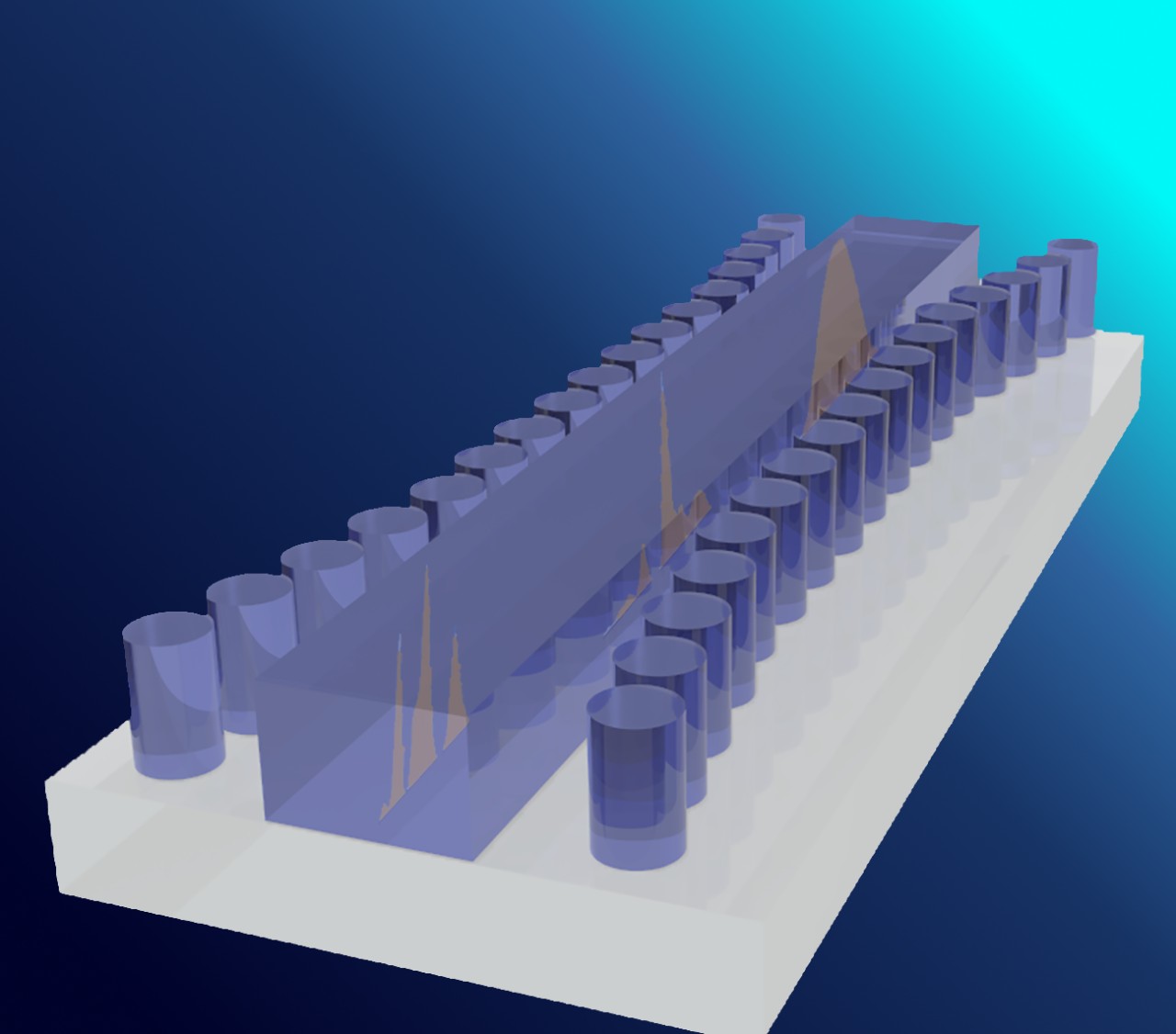
A tsunami holds its wave shape over very long distances across the ocean, retaining its power and ‘information’ far from its source.
In communications science, retaining information in an optic fibre that spans continents is vital. Ideally, this requires the manipulation of light in silicon chips at the source and reception end of the fibre without altering the wave shape of the photonic packet of information. Doing so has eluded scientists until now.
A collaboration between the University of Sydney Nano Institute and Singapore University of Technology and Design has for the first time manipulated a light wave, or photonic information, on a silicon chip that retains its overall ‘shape’.
Such waves – whether a tsunami or a photonic packet of information – are known as ‘solitons’. The Sydney-Singapore team has for the first time observed ‘soliton’ dynamics on an ultra-silicon-rich nitride (USRN) device fabricated in Singapore using state-of-the-art optical characterisation tools at Sydney Nano.
This foundational work, published today in Laser & Photonics Reviews, is important because most communications infrastructure still relies on silicon-based devices for propagation and reception of information. Manipulating solitons on-chip could potentially allow for the speed up of photonic communications devices and infrastructure.
Ezgi Sahin, a PhD student at SUTD conducted the experiments with Dr Andrea Blanco Redondo at the University of Sydney.
“The observation of complex soliton dynamics paves the way to a wide range of applications, beyond pulse compression, for on-chip optical signal processing,” Ms Sahin said. “I’m happy to be a part of this great partnership between the two institutions with deep collaboration across theory, device fabrication and measurement.”
Co-author of the study and Director of Sydney Nano, Professor Ben Eggleton, said: “This represents a major breakthrough for the field of soliton physics and is of fundamental technological importance.
“Solitons of this nature – so-called Bragg solitons – were first observed about 20 years ago in optical fibres but have not been reported on a chip because the standard silicon material upon which chips are based constrains the propagation. This demonstration, which is based on a slightly modified version of silicon that avoids these constraints, opens the field for an entirely new paradigm for manipulating light on a chip.”
Professor Dawn Tan, a co-author of the paper at SUTD, said: “We were able to convincingly demonstrate Bragg soliton formation and fission because of the unique Bragg grating design and the ultra-silicon-rich nitride material platform (USRN) we used. This platform prevents loss of information which has compromised previous demonstrations.”
Bragg Soliton Compression and Fission on CMOS‐Compatible Ultra‐Silicon‐Rich Nitride
Ezgi Sahin, Andrea Blanco‐Redondo, Peng Xing, Doris K. T. Ng, Ching E. Png, Dawn T. H. Tan, Benjamin J. Eggleton
Laser & Photonics Reviews 2019
DOI: https://doi.org/10.1002/lpor.201900114
Contact information:
Professor Ben Eggleton
Director of University of Sydney Nano Institute
benjamin.eggleton@sydney.edu.au
Tel: +61 2 9351 3604
Fax: +61 2 9351 7726
Lab: Photonics and Optical Physics group
Professor Dawn Tan
Singapore University of Technology and Design (SUTD)
dawn_tan@sutd.edu.sg
Tel: +65 6499 4607
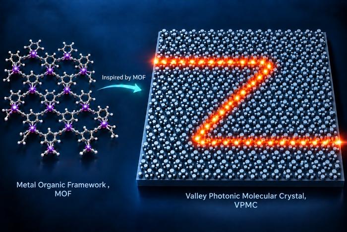
Inspired by Metal-Organic Framework based topological insulators, researchers at Tsinghua University proposed valley photonic molecular crystal (VPMC) and investigated the impact of molecular rotation on the valley-topological properties of VPMC. Credit: Tsinghua University/Xue Feng A research team led by Yidong Huang at Tsinghua University, including Xue Feng and Yongzhuo Li, has developed valley photonic molecular crystals (VPMCs) on a silicon platform. Combining theoretical modeling,...
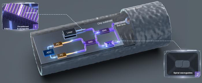
The system integrates a III-V semiconductor light source, SiN-based interferometers, Si-Ge photodetectors (PDs), and an integrated ball-lens microprobe, thereby combining the distinct advantages of multiple photonic integration platforms. The insets illustrate complementary technologies that can be incorporated to realize a miniaturized, fully integrated OCT system. Abbreviations: ADC, analog-to-digital converter. Inset 1: Foundry-scalable embedded III-V lasers on silicon-on-insulator (SOI)...

From left to right: Three photons with different quantum states enter an interferometer with three beam splitters. At each beam splitter, they can take different paths at the same time in superposition. The researchers then measured how often the three photons ended up together at the same output. Counterintuitively, it is possible to make the photons more similar to each other and at the same make them less likely to “bunch” together. AI-generated illustration, by Leonardo Novo. We usually...
