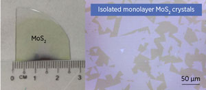
Mass production of large, uniform sheets of single-layer molybdenum disulfide, MoS2, is difficult, which limits its commercial application. A*STAR researchers have modified an existing manufacturing technique to enable the use of MoS2 in a range of technologies from photodevices to flexible, transparent sensors.
The two-dimensional material has attracted considerable attention because of its extraordinary physical, electronic and optoelectronic properties, including flexibility, transparency and semiconducting characteristics. But fabricating large-scale, defect-free single layers of MoS2 is highly challenging.
Dongzhi Chi and his team from the A*STAR Institute of Materials Research and Engineering, in collaboration with colleagues from the National University of Singapore and the Indian Institute of Science Education and Research, has modified a current technique, known as chemical vapor deposition (CVD), so that it can now produce uniform, centimeter-sized sheets of MoS2 crystals with large grain sizes.
“The physical properties of MoS2 vary greatly with its thickness,” explains Chi, “to maintain its remarkable electronic and physical properties we need a method that can uniformly deposit MoS2 films over a large area with high crystallinity.”
Although CVD is an effective technique for fabricating large-area, uniform sheets of MoS2 of varying thickness on different substrates, and significant progress has been made in improving the quality of MoS2 monolayers produced by the technique, little attention has been paid to controlling the chemical vapors using physical barriers during the growth of MoS2 crystals.
By introducing a nickel oxide (NiO) barrier, the researchers were able to control the concentration and distribution of chemical vapors during the growth of MoS2 crystals. Because NiO reacts with molybdenum trioxide (MoO3), one of the chemical reactants used in the growth process, it traps and lowers the MoO3 concentration, allowing the uniform deposition of monolayers of MoS2 over a large area.
“The advantage of this approach is the ease of implementation as well as a reduction in contamination, and it allows for control of the chemical exposure during the growth process,” says Chi.
The work has led to further advances in the fabrication of uniform and large-area MoS2 monolayers, and could also be applied to other two-dimensional materials.
“We are now looking to scale up our fabrication process for producing even larger sheets, which could pave the way for next-generation optoelectronic and sensor technologies,” says Chi.
Modification of Vapor Phase Concentrations in MoS2 Growth Using a NiO Foam Barrier
Yee-Fun Lim, Kumar Priyadarshi, Fabio Bussolotti, Pranjal Kumar Gogoi, Xiaoyang Cui, Ming Yang, Jisheng Pan, Shi Wun Tong, Shijie Wang, Stephen J. Pennycook, Kuan Eng Johnson Goh, Andrew T. S. Wee, Swee Liang Wong, and Dongzhi Chi
ACS Nano, 2018, 12 (2), pp 1339–1349
DOI: 10.1021/acsnano.7b07682
A*STAR Institute of Materials Research and Engineering
#2DMaterials #MaterialScience
SPECS reports on work at the LMA microscopy lab, where Dr. David Serrate's team used the JT-STM to study graphene nanoribbons on MgO/Ag(001) and the Aarhus 150 to monitor nanostructure growth.
Nanologica's board has resolved on a rights issue of units of appx. SEK 110.5 million, with an oversubscription option of up to SEK 10 million. Commitments and a guarantee intention cover appx. SEK 85.7 million.
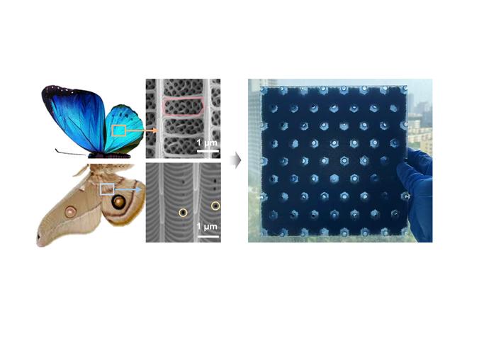
Researchers at Harbin Institute of Technology have printed a 24 mm metamaterial that absorbs impact, shields microwaves and damps low-frequency noise at once. Inspired by butterfly wing scales, it nests a gyroid lattice inside a hexagonal honeycomb, absorbing 21.9 times more impact energy than an equal-weight honeycomb and capturing over 90% of 2-40 GHz radiation and 600-900 Hz sound.
This week in nanotech
$108.5M raised
8 funding rounds · 46 deals tracked
New products
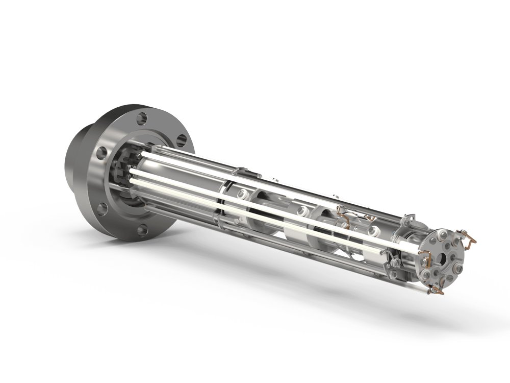 DLS-1 Mass Spectrometer for Fusion Gas AnalysisHiden Analytical Featured
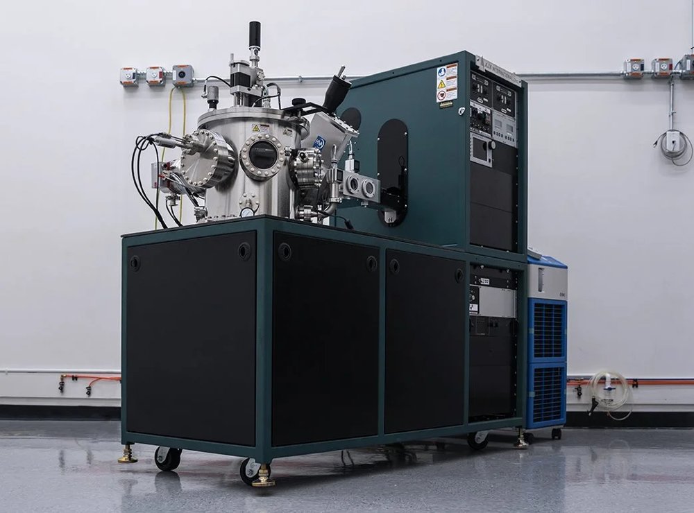 Orion Sputtering Deposition SystemsAJA International Featured
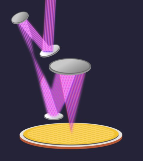 Aether®Lam Research
Market insights
Last 30 days: Quantum Technologies drew the most money: $3.17B.
Money raised per month