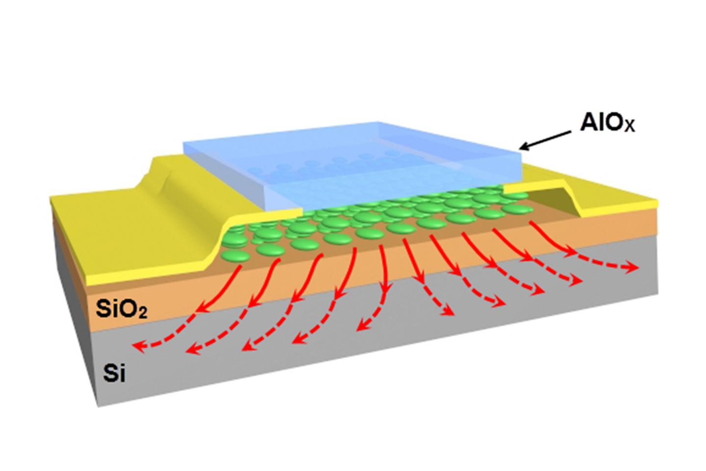
Sandwiching two-dimensional materials used in nanoelectronic devices between their three-dimensional silicon bases and an ultrathin layer of aluminum oxide can significantly reduce the risk of component failure due to overheating, according to a new study published in the journal of Advanced Materials led by researchers at the University of Illinois at Chicago College of Engineering.
Many of today's silicon-based electronic components contain 2D materials such as graphene. Incorporating 2D materials like graphene -- which is composed of a single-atom-thick layer of carbon atoms -- into these components allows them to be several orders of magnitude smaller than if they were made with conventional, 3D materials. In addition, 2D materials also enable other unique functionalities. But nanoelectronic components with 2D materials have an Achilles' heel -- they are prone to overheating.
This is because of poor heat conductance from 2D materials to the silicon base.
"In the field of nanoelectronics, the poor heat dissipation of 2D materials has been a bottleneck to fully realizing their potential in enabling the manufacture of ever-smaller electronics while maintaining functionality," said Amin Salehi-Khojin, associate professor of mechanical and industrial engineering in UIC's College of Engineering.
One of the reasons 2D materials can't efficiently transfer heat to silicon is that the interactions between the 2D materials and silicon in components like transistors are rather weak.
"Bonds between the 2D materials and the silicon substrate are not very strong, so when heat builds up in the 2D material, it creates hot spots causing overheat and device failure," explained Zahra Hemmat, a graduate student in the UIC College of Engineering and co-first author of the paper.
In order to enhance the connection between the 2D material and the silicon base to improve heat conductance away from the 2D material into the silicon, engineers have experimented with adding an additional ultra-thin layer of material on top of the 2D layer -- in effect creating a "nano-sandwich" with the silicon base and ultrathin material as the "bread."
"By adding another 'encapsulating' layer on top of the 2D material, we have been able to double the energy transfer between the 2D material and the silicon base," Salehi-Khojin said.
Salehi-Khojin and his colleagues created an experimental transistor using silicon oxide for the base, carbide for the 2D material and aluminum oxide for the encapsulating material. At room temperature, the researchers saw that the conductance of heat from the carbide to the silicon base was twice as high with the addition of the aluminum oxide layer versus without it.
"While our transistor is an experimental model, it proves that by adding an additional, encapsulating layer to these 2D nanoelectronics, we can significantly increase heat transfer to the silicon base, which will go a long way towards preserving functionality of these components by reducing the likelihood that they burn out," said Salehi-Khojin. "Our next steps will include testing out different encapsulating layers to see if we can further improve heat transfer."
Enhanced Thermal Boundary Conductance in Few‐Layer Ti3C2 MXene with Encapsulation
Poya Yasaei, Zahra Hemmat, Cameron J. Foss, Shixuan Justin Li, Liang Hong, Amirhossein Behranginia Leily Majidi, Robert F. Klie, Michel W. Barsoum, Zlatan Aksamija, Amin Salehi‐Khojin
Advanced Materials, First published: 04 September 2018
DOI: https://doi.org/10.1002/adma.201801629
Contact information:
Prof. Amin Salehi-Khojin
UIC's College of Engineering, Mechanical & Industrial Engineering
salehikh@uic.edu
Tel: (312) 413-1523
URL: http://nanomaterialsenergysystems.engr.uic.edu/
University of Illinois at Chicago (UIC)
#Nanoelectronics #2DMaterials #Silicon
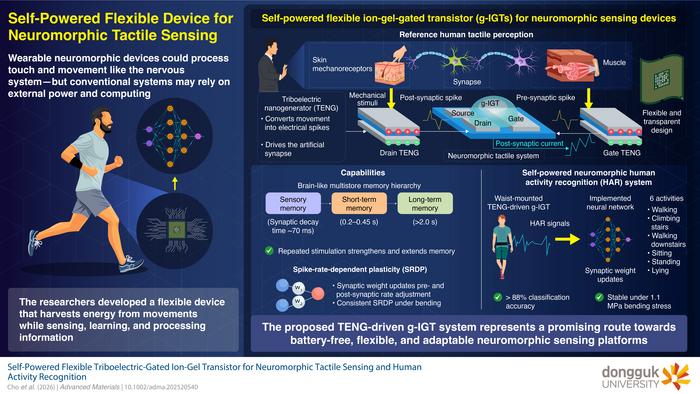
The proposed TENG-driven g-IGT is a flexible, self-powered neuromorphic device capable of reproducing multiple memory states and spike-rate-dependent learning Neuromorphic devices, which are designed to emulate aspects of biological neural networks, are promising candidates for developing low-power and intelligent sensing technologies, including wearable applications. Among the device architectures explored for neuromorphic computing, graphene-channel ion-gel-gated transistors (g-IGTs) are...
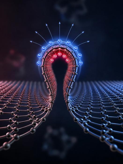
Rice University researchers have shown that sub-nanometer wrinkles in graphene generate flexoelectric charge separation, reshaping local electrical behavior through curvature alone. Extreme bending produces polarization far stronger than in larger systems and may enable geometry-controlled electronics without chemical doping. Published in Advanced Materials.
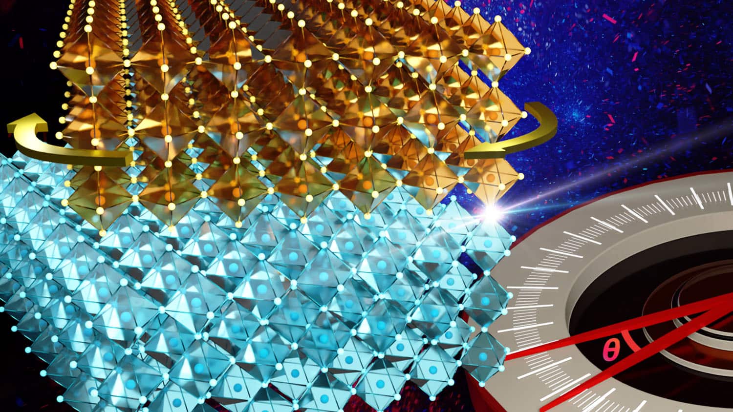
Researchers at NC State have extended twistronics beyond van der Waals materials into strongly bonded crystalline oxides. By stacking sodium niobate membranes with twist angles controlled down to 0.1 degrees, and confirming results via synchrotron X-ray diffraction, the team found interlayer bonds distort the atomic lattice, shifting phase structure and domain configuration. The technique works at near-millimeter scale, far larger than typical twistronic devices, marking a real step toward pract
