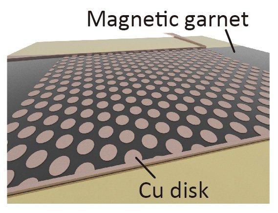
A collaborative group of researchers has potentially developed a means of controlling spin waves by creating a hexagonal pattern of copper disks on a magnetic insulator (shown in Figure 1). The breakthrough is expected to lead to greater efficiency and miniaturization of communication devices in fields such as artificial intelligence and automation technology.
Details of the study were published in the journal Physical Review Applied on January 30, 2024.
In a magnetic material, the spins of electrons are aligned. When these spins undergo coordinated movement, it generates a kind of ripple in the magnetic order, dubbed spin waves. Spin waves generate little heat and offer an abundance of advantages for next-generation devices.
Implementing spin waves in semiconductor circuits, which conventionally rely on electrical currents, could lessen power consumption and promote high integration. Since spin waves are waves, they tend to propagate in random directions unless controlled by structures and other means. As such, elements capable of generating, propagating, superimposing, and measuring spin waves are being competitively developed worldwide.
"We leveraged the wavelike nature of spin waves to successfully control their propagation directly," points out Taichi Goto, associate professor at Tohoku University's Electrical Communication Research Institute, and co-author of the paper. "We did so by first developing an excellent magnetic insulator material called magnetic garnet film, which has low spin wave losses. We then periodically arranged small copper disks with diameters less than 1 mm on this film."
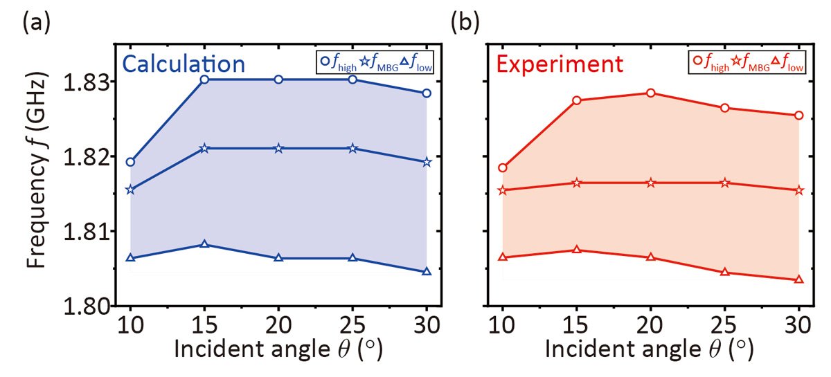
By arranging copper disks in a hexagonal pattern resembling snowflakes, Goto and his colleagues could effectively reflect the spin waves. Furthermore, by rotating the magnonic crystal (shown in Figure 2) and changing the incident angle of spin waves, the researchers revealed that the frequency at which the magnonic band gap occurs remains largely unchanged in the range from 10 to 30 degrees. This suggests the potential for the two-dimensional magnonic crystal to freely control the propagation direction of spin waves.
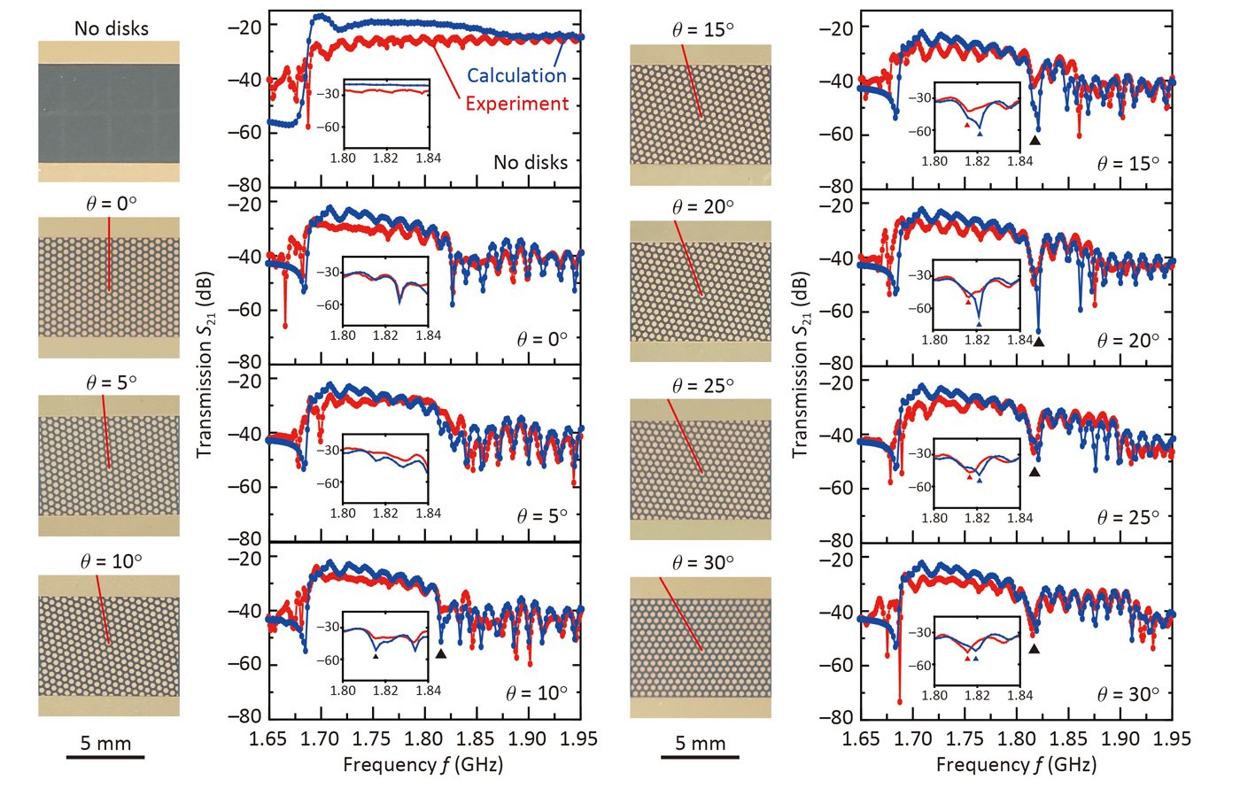
Goto notes the novelty of their findings: "To date, there have been no experimental confirmations of changes in the spin wave incident angle for a two-dimensional magnonic crystal comprising a magnetic insulator and copper disks, making this the world's first report."
Looking ahead, the team hopes to demonstrate the direction control of spin waves using two-dimensional magnonic crystals and to develop functional components that utilize this technology.
Reference
Orientation-dependent two-dimensional magnonic crystal modes in an ultralow-damping ferrimagnetic waveguide containing repositioned hexagonal lattices of
Cu disks
Kanta Mori, Takumi Koguchi, Toshiaki Watanabe, Yuki Yoshihara, Hibiki Miyashita, Dirk Grundler, Mitsuteru Inoue, Kazushi Ishiyama, and Taichi Goto
https://journals.aps.org/prapplied/abstract/10.1103/PhysRevApplied.21.014061
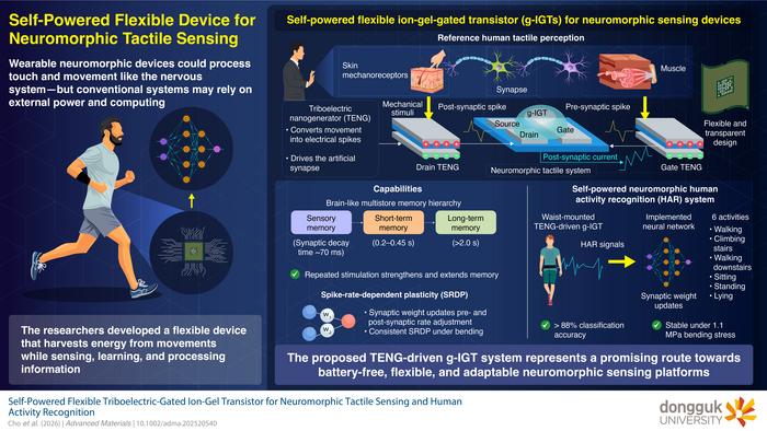
The proposed TENG-driven g-IGT is a flexible, self-powered neuromorphic device capable of reproducing multiple memory states and spike-rate-dependent learning Neuromorphic devices, which are designed to emulate aspects of biological neural networks, are promising candidates for developing low-power and intelligent sensing technologies, including wearable applications. Among the device architectures explored for neuromorphic computing, graphene-channel ion-gel-gated transistors (g-IGTs) are...
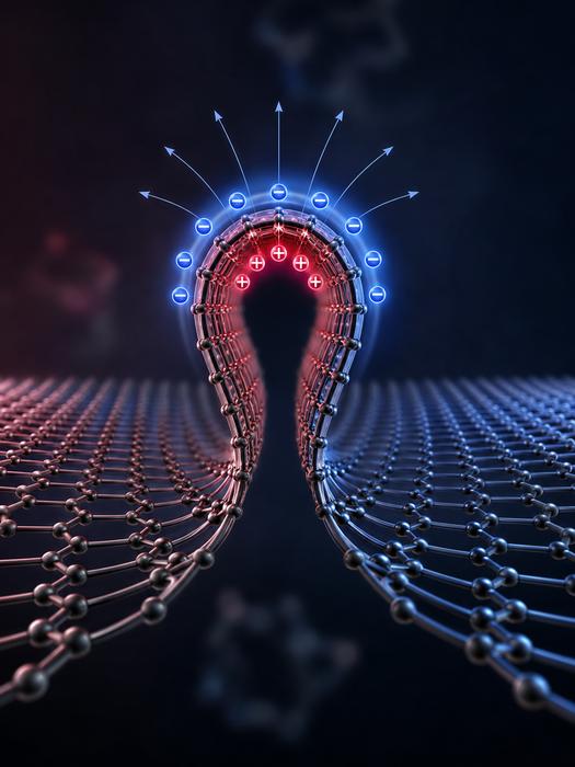
Rice University researchers have shown that sub-nanometer wrinkles in graphene generate flexoelectric charge separation, reshaping local electrical behavior through curvature alone. Extreme bending produces polarization far stronger than in larger systems and may enable geometry-controlled electronics without chemical doping. Published in Advanced Materials.
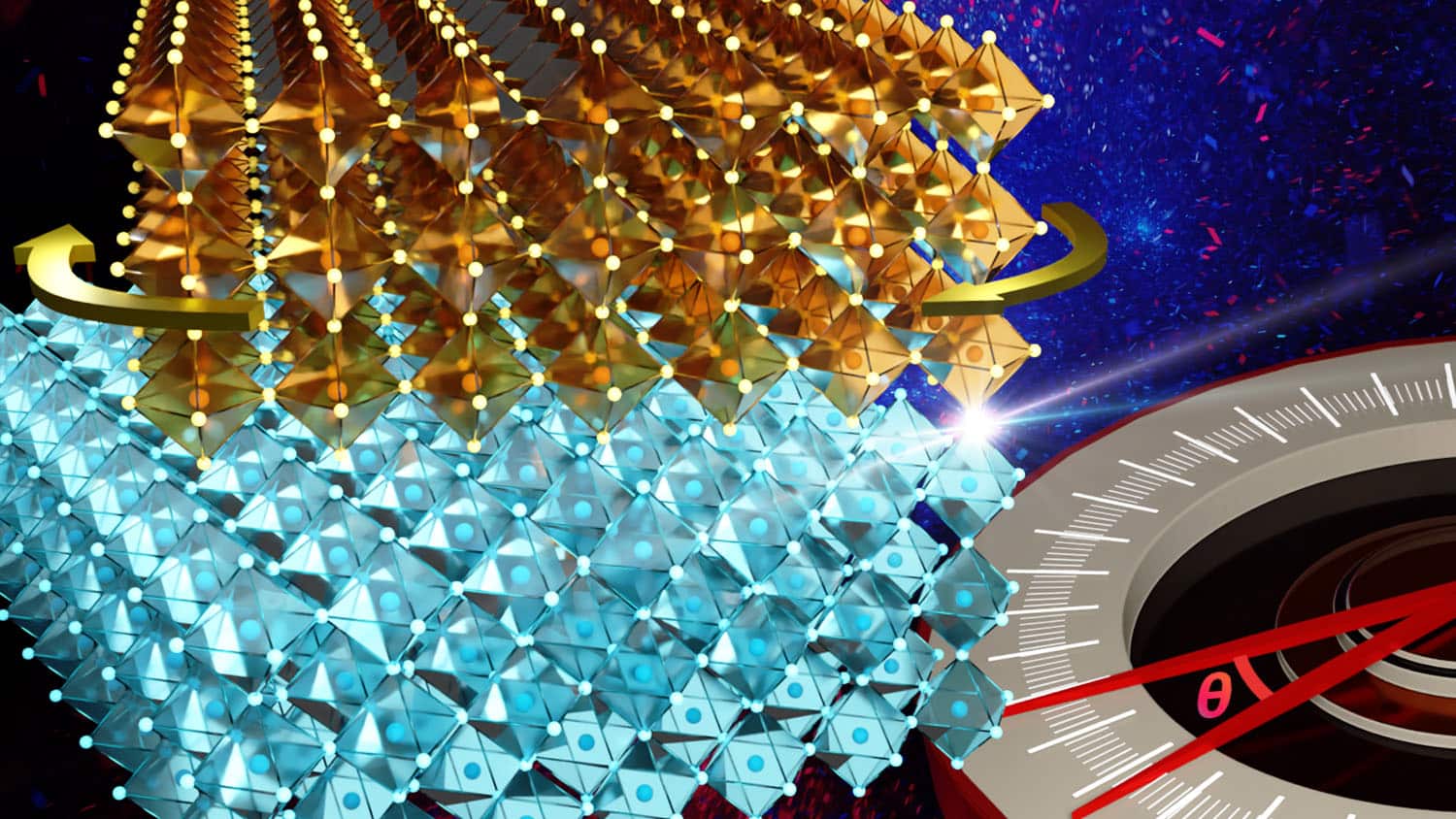
Researchers at NC State have extended twistronics beyond van der Waals materials into strongly bonded crystalline oxides. By stacking sodium niobate membranes with twist angles controlled down to 0.1 degrees, and confirming results via synchrotron X-ray diffraction, the team found interlayer bonds distort the atomic lattice, shifting phase structure and domain configuration. The technique works at near-millimeter scale, far larger than typical twistronic devices, marking a real step toward pract
