The work methodology in a theoretical group often implies discussions in front of the data to elucidate what is the story the nature is trying to tell us. One day, an interesting revelation took place at IMDEA Nanociencia institute in Madrid.
Dr. Pierre Pantaleón, researcher at the Group of Theoretical Modelling at IMDEA Nanociencia, was discussing with Prof. Paco Guinea - the leader of the Group- about strained bilayer graphene, it is, two layers of graphene piled on top of each other and slightly stretched out by a small force. Pierre, a meticulous researcher with a penchant for visual aids, was showing the group his animated visualization of strained graphene when Paco noticed an anomaly that had escaped everyone else’s scrutiny. As it turns out, when bilayer graphene goes under strain, its Brillouin zone (the unit cell in the momentum space) is distorting, and eventually, collapsing in one direction. This distortion at the collapsing point caused an error in Pierre's visualization programme suggesting the presence of some kind of singularity.
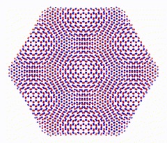
In Physics, singularities, like the one the researchers were observing, demand careful consideration. They could indicate something may be amiss, shifting, or simply necessitating a closer examination. By that time, Dr. Andreas Sinner, a brilliant theoretical physicist currently working on Opole University on Poland, joined Paco’s research group and started looking together with Pierre on the origin of this singularity. It was the concurrent transformation in real space that truly captivated their attention: strained graphene gave rise to the emergence of almost perfect one-dimensional moiré patterns —one-dimensional channels— within the 2-dimensional material.
Previously, scientists had glimpsed such phenomena through microscopes and had regarded them as design errors such as dislocations or adhered materials. See for example the work of McEuen (Cornell Uni.), Mendoza (Rio de Janeiro Uni) or Zhu (Columbia Uni.). But behind what appeared to be artifacts were masked effects the researchers describe now. The research team at IMDEA Nanociencia confirms that this is a natural occurrence within hexagonal honeycomb lattices -like those of graphene- specifically taking place when two layers are stacked at a slight twist angle, and strain is applied.
The most significant contribution of the researchers lies in their discovery of analytical solutions for the critical strain required to generate these one-dimensional channels. Surprisingly, this solution is beautifully simple, relying on just two variables: the twist angle and the Poisson ratio—a material-specific constant. Their findings lead them to obtain a single mathematical formula to describe the phenomenon, and this formula gives us information on the physical origin.
The physics described in their work, published in Physical Review Letters, is not new, but the explanation of the phenomenon in such simple terms –single analytical expression- is elegant and unique. The findings open the door to engineering novel materials on surfaces capable of featuring these one-dimensional channels. Within these channels, electrons find themselves confined, in contrast to the free movement they exhibit in the standard 2D graphene landscape. Electrons within these channels exhibit a preferential direction of movement.
The implications of this discovery are vast, with potential applications extending to other materials, such as dichalcogenides, and can be extended to other geometric configurations as well.
The Group of Prof. Guinea is actively investigating the possibilities of graphene, in twisted and non-twisted bilayers, that includes the observation of superconductivity. A comprehensive review was published recently in Nature Reviews Physics.
Reference
Strain-Induced Quasi-1D Channels in Twisted Moiré Lattices
Andreas Sinner, Pierre A. Pantaleón, and Francisco Guinea
https://journals.aps.org/prl/abstract/10.1103/PhysRevLett.131.166402
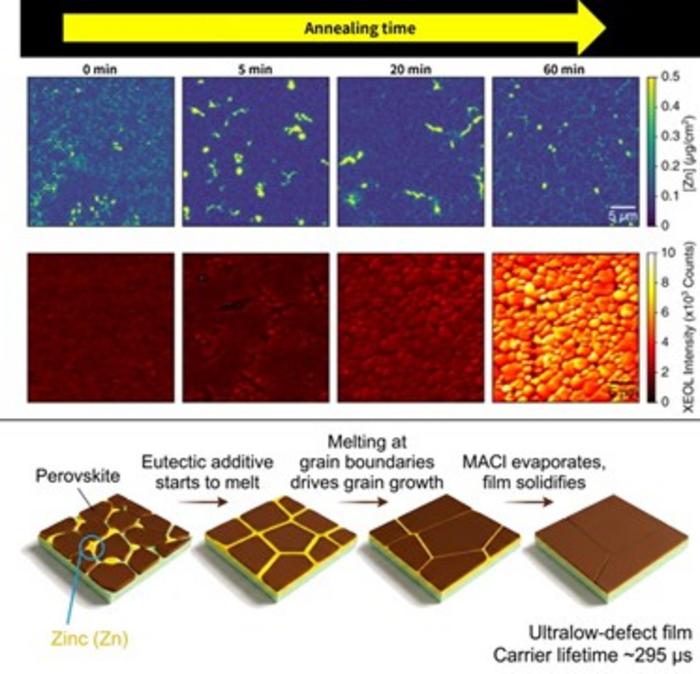
A eutectic mixture of methylammonium chloride and a zinc halide melts at about 100 degrees Celsius, forming a transient liquid layer at perovskite grain boundaries that lets crystals merge into larger, cleaner grains. The resulting films reached a carrier lifetime of roughly 295 microseconds and a surface recombination velocity of 0.3 cm/s, the lowest reported for lead halide perovskites.
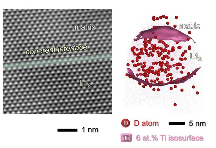
Researchers at the University of Sydney have directly observed hydrogen dissolved in the interstitial spaces between metal atoms in alloys, a world first. Using cryogenic atom probe tomography with deuterium tracers, electron microscopy and theoretical calculations, the team showed hydrogen occupies sites between atoms rather than only collecting at defects, and that local atomic arrangement and chemistry dictate where it prefers to reside.
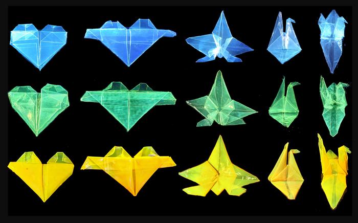
Researchers have developed carbon dots whose fluorescence shifts across the visible spectrum, from blue to red, depending on concentration, liquid environment and acidity. By tuning the particles' surfaces, the team produced versions that change color reversibly as pH shifts, then incorporated them into polymer powders, molded shapes and flexible films.
This week in nanotech
$13.6M raised
3 funding rounds · 20 deals tracked
New products
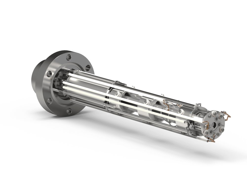 DLS-1 Mass Spectrometer for Fusion Gas AnalysisHiden Analytical Featured
 Ti-WCMBN Nanomaterialia Featured
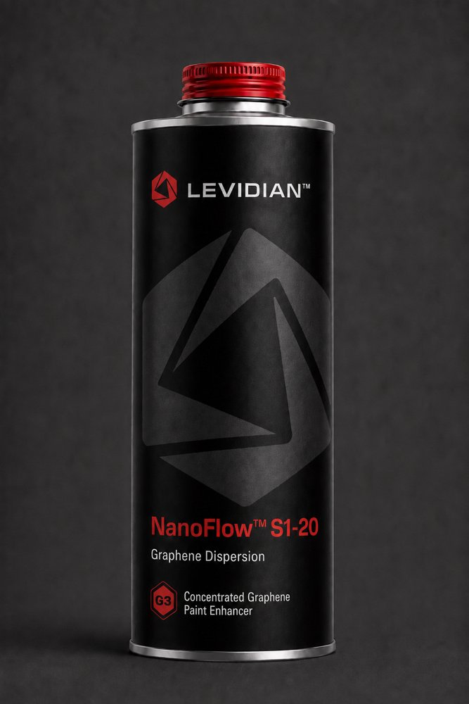 NanoFlow® S1-20Levidian
Market insights
Last 30 days: Quantum Technologies was the busiest vertical: 61 of 192 events (32%).
Money raised per month