
The mysterious changes in phases of matter – from solid to liquid and back again – have fascinated Eun-Ah Kim since she was in lower elementary school in South Korea. Without cold drinking water readily available, on hot days the children would bring bottles of frozen water to school.
Kim noticed that when the water melted, the volume changed.
“That revealed to me there is something in there that I cannot see with my eyes,” said Kim, professor of physics in the College of Arts and Sciences. “Matter around me is made up of invisible entities that interact and do something together to change their state.”
Kim’s fascination with melting continues, but she now studies transitions in more exotic materials than water: electron crystals. In a new paper, Kim and first author Michael Matty, M.S. ’19, Ph.D. ’22, have described a phase in between the liquid and the solid for these electron structures – a liquid crystal state.
Their paper, “Melting of Generalized Wigner Crystals in Transition Metal Dichalcogenide Heterobilayer Moiré Systems,” published Nov. 19 in Nature Communications.
Because electrons are all negatively charged, they repel each other; thus their preferred state is to be as far as possible from every other electron in the material that contains them. The regular arrangement of electrons that results from this equal repulsion in all directions is called a Wigner crystal.
Kim and Matty wanted to know how the electrons transition from one regular arrangement as a crystal to another regular arrangement as a crystal, or how they “melt.”
To find the answer, the researchers studied how electrons interact on an artificial grid, called a moiré lattice, formed by placing two distinct atomically thin materials on top of each other. Because they are on a grid rather than a smooth surface, the electrons can’t choose arbitrary locations away from each other, but must fill a point on the grid; the grid constrains how they are arranged.
“When the grid is partially filled, we get to see the impact of their repulsion and how strongly the electrons are interacting with each other,” Kim said. “As a result of their interaction, we see that they occupy a regular interval of sites on the lattice, not random intervals.”
The particular moiré lattice the researchers considered for their study was developed by Cornell experimentalists Kin Fai Mak, professor of physics (A&S) and associate professor of physics in Cornell Engineering, and Jie Shan, professor of physics (A&S) and applied and engineering physics (Engineering).
“Cornell experimentalists are at the frontier of artificial moiré material research,” Kim said, “doing these amazing experiments with an astonishing degree of control, offering opportunities for theoretical ideas to manifest in physical systems.”
Shan and Mak had experimentally detected particular rigid structures that the electrons formed in partially filled grids. Kim and Matty studied how one of these structures would transition to another. They found that when conditions were changed, that very regular, rigid array becomes more fluid.
The researchers identified an intermediate phase between solid and liquid in electrons that has some regularity but not as much as a solid, and not as much freedom as a liquid. They found that the electrons in this state arrange themselves into tiny strips that can move around and orient themselves in structures.
“Electronic liquid crystals had been discussed theoretically, but we’re providing a visual image of how they can form microscopically: four or five electrons forming a piece that can be arranged,” said Kim. “What we’ve accomplished is a microscopic understanding of what was only known in principle to be possible.”
Reference
Melting of generalized Wigner crystals in transition metal dichalcogenide heterobilayer Moiré systems
Michael Matty & Eun-Ah Kim
https://www.nature.com/articles/s41467-022-34683-x
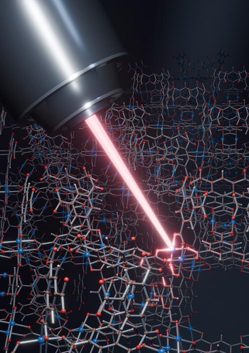
Filling the pores of a copper-based metal-organic framework with imidazolium ionic liquids makes the fragile material hard enough to pattern at room temperature. Treated Cu3BTC2 resisted the crystal damage seen in untreated samples during focused gallium ion beam etching, and researchers produced lines just 130 to 300 nanometres wide. The liquids appear to absorb heat and dissipate charge, and also raised hardness and thermal stability.
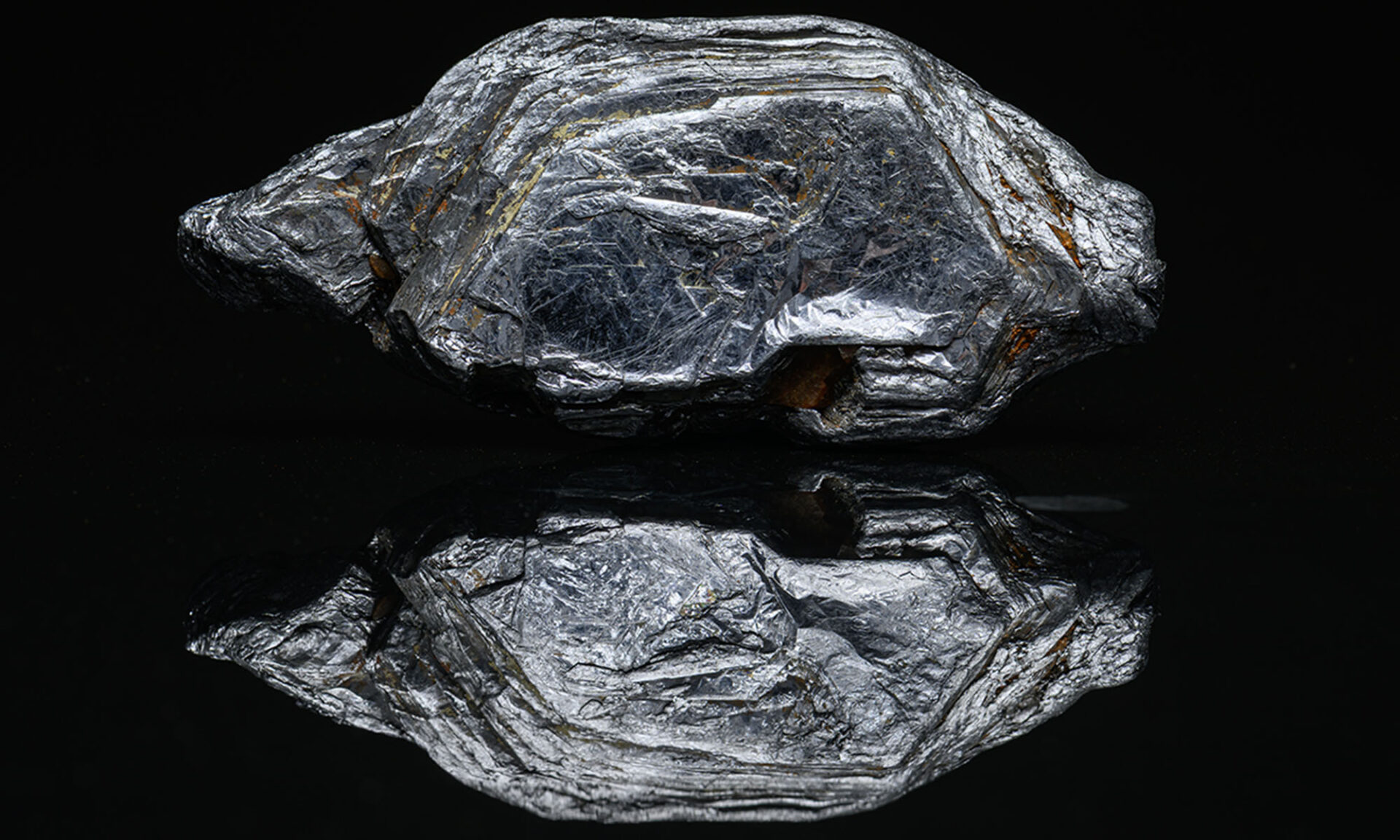
Engineers at the University of Rochester and Technion found that pressing a diamond nanoindenter tip a few nanometers into molybdenum can recrystallize the heat-resistant metal at room temperature, a process normally requiring about 1,000 degrees Celsius. Stopping the test just after the pop-in event reforms crystal grains in a tiny region around the dent, offering a way to repair defects and tailor properties locally.
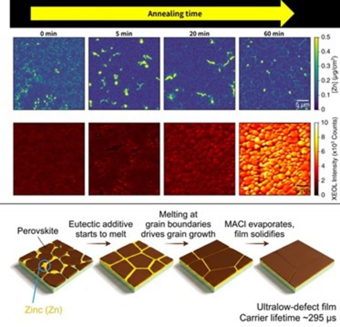
A eutectic mixture of methylammonium chloride and a zinc halide melts at about 100 degrees Celsius, forming a transient liquid layer at perovskite grain boundaries that lets crystals merge into larger, cleaner grains. The resulting films reached a carrier lifetime of roughly 295 microseconds and a surface recombination velocity of 0.3 cm/s, the lowest reported for lead halide perovskites.
This week in nanotech
9 deals tracked
New products
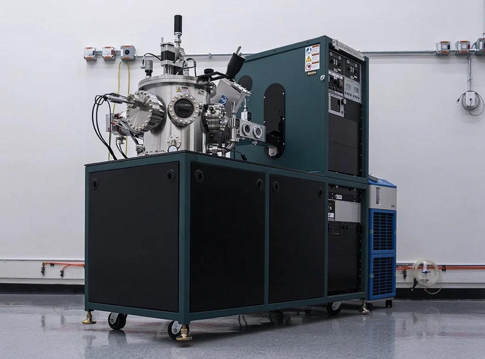 Orion Sputtering Deposition SystemsAJA International Featured
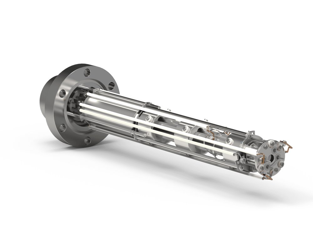 DLS-1 Mass Spectrometer for Fusion Gas AnalysisHiden Analytical Featured
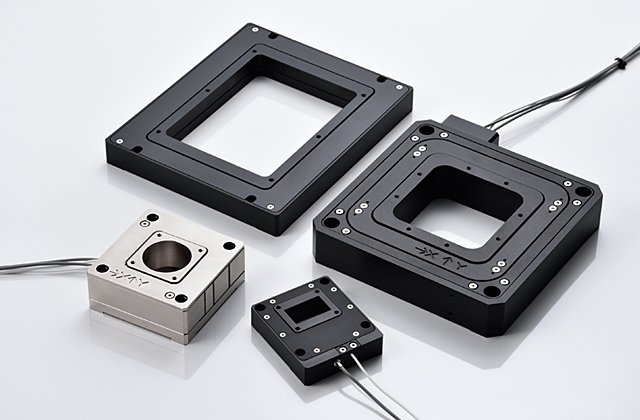 PKVH / PKVL ZAxis With an opening modelTHK PRECISION CO.,LTD.
Market insights
Last 30 days: Semiconductors & Electronics drew the most money: $545M.
Money raised per month