Rice University
A new chip-making technique exploits a material’s crystal structure to create nanoscale patterns at room temperature directly onto hard materials used in devices, including silica. The method could make it easier to pattern chips relaying both electronic- and light-based signals, helping advance next-generation photonic and optoelectronic devices.
Materials scientists at Rice University used alpha-molybdenum trioxide, a semiconducting crystal whose atomic structure exhibits a property called anisotropy, meaning that it behaves differently depending on the direction inside the material. When hit with an electron beam, the material deforms, creating a pattern of nanoscale ripples. The researchers showed this response could be used to pattern silica and other hard materials used in electronics.
According to a study published in Nature Communications, the research team placed a layer of the anisotropic crystal on top of silica and irradiated the two with an electron beam. This caused the alpha-molybdenum trioxide to buckle under the stress, while at the same time softening the silica underneath.
“Under an electron beam, the atomic bond in silica can rearrange, so the material can slowly deform even at room temperature,” said Hae Yeon Lee, an assistant professor of materials science and nanoengineering at Rice and a corresponding author on the study. “The challenge is that silica does not deform by itself under the beam ⎯ it also needs a stress source. Our idea was to use the alpha-molybdenum trioxide as the stress source.”
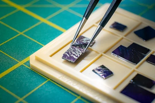
The researchers exposed the material to an electron beam, which gave rise to directional stress resulting in an organized pattern, with rows of evenly spaced ripples that lined up with the crystal’s internal structure.
“In this work, we translate atomic scale anisotropy into hundreds of nanometer scale wrinkles,” Lee said.
The ripples are far smaller than the width of a human hair and can bend and split light, much like the grooves on a CD create rainbow colors. That makes them useful as optical gratings, structures that guide light on a chip.
Hard materials tend to crack or form random defects in response to mechanical stress-based patterning. So even while wrinkle-based patterning techniques can produce nanoscale structures without the complex manufacturing involved in standard chip fabrication, using them was generally thought to necessitate soft, elastic substrates.
The Rice team’s work demonstrates a new way to deploy wrinkle-based patterning on rigid insulating materials. Moreover, patterns can be tuned by changing the thickness of the anisotropic layer or the intensity of the electron beam.
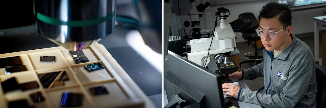
“This work is useful because conventional methods for making nanoscale wrinklelike patterns often require many fabrication steps, high cost and chemical processing that can leave residue on the surface of the chip,” Lee said. “With our method, the wrinkles are created in one simple step at room temperature.”
After the patterning is achieved, the alpha-molybdenum trioxide layer can simply be peeled off the silica. The researchers observed similar effects on other common insulating materials, including aluminum oxide and silicon nitride, suggesting the method could work broadly across materials already used in semiconductor manufacturing.
The ability to create optical structures directly on standard chip materials could offer a simpler route toward integrating light-based technologies into future devices.
Reference
Room temperature molding of amorphous dielectrics via van der Waals anisotropy at the nanoscale | Yifeng Liu, Zhengjie Huang, Xinyan Li, Chen-yang Lin, Aryan Chugh, Tian Lang, Kenji Watanabe, Takashi Taniguchi, Jun Lou, Yanfei Gao, Yimo Han, Xuedan Ma and Hae Yeon Lee

UCSB and UMass Amherst researchers have demonstrated the first chip-scale, stabilized visible-light Brillouin laser that drives a trapped-ion optical clock and qubit at room temperature. The compact photonic platform achieves 99.6% SPAM fidelity with fewer pulses than table-top systems, enabling portable, scalable quantum computing, sensing, and precision timing.

Optical waveguide microresonators on a chip created in this effort, which are ten times thinner than human hair. @CU Boulder College of Engineering and Applied Science CU Boulder researchers have built high performing optical microresonators opening the door for new sensor technologies. At its simplest form, a microresonator is a tiny device that can trap light and build up its intensity. Once the intensity is high enough, researchers can perform unique light operations. “Our work is about...

Although quantum technology holds great promise for enabling faster computing, more secure communication and new types of sensing, different quantum systems often don’t interact well with each other. To address this, engineers have developed platforms based on a type of phonon known as a surface acoustic wave. However, the limited propagation distance due to high loss and inherently open 2D structure of existing solutions make such devices relatively large, posing a barrier to their practical...