ICFO-Institut de Ciencies Fotoniques
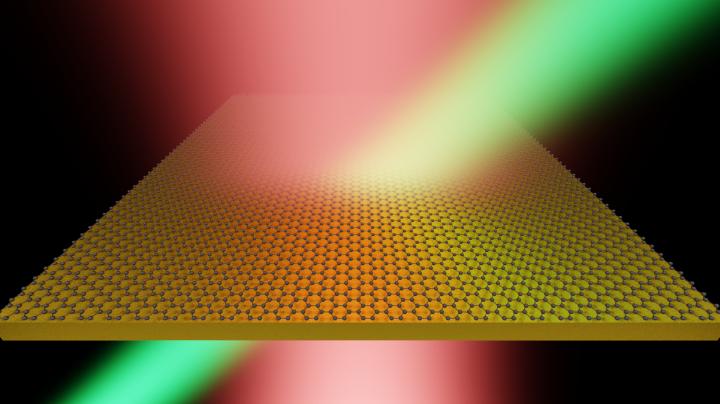
Surface plasmons in graphene have been widely studied in the past decade due to their very appealing properties, such as the strong tunability of its optical properties through electrical gating and the relatively high plasmon lifetime. However, these exceptional properties are limited to lower frequencies ranging from the mid-infrared (mid-IR) to the terahertz (THz) spectral regions. Additionally, electrical tunability of graphene cannot be achieved in an ultrafast manner, what poses an obstacle for its application in high-speed technological devices that are becoming increasingly important.
In a new paper published in Light Science & Application, a team from ICFO-Institut de Ciencies Fotoniques (Barcelona, Spain) has proposed an all-optical technique to modulate the plasmonic response of graphene- and/or thin-metal-based systems in an ultrafast manner, in a spectrum ranging from mid-infrared to visible (vis-NIR) frequencies. They propose a pump-probe setup where an ultrafast and very intense pump beam is used to heat the electrons of the graphene. Based on the low heat capacity of this 2D material -meaning that a small amount of energy absorbed by this material can induce a large increase in the temperature of its electrons- and on the strong dependence of graphene's conductivity with its electronic temperature, the optical properties of the system will be modulated by the electronic temperature increase, and this can be measured by the probe beam.
Interestingly, this technique can be used to all-optically excite plasmons not only in the graphene sheet, but also in a thin metallic layer placed nearby it. Following a previous work by the same group, they propose to do so by engineering a pump beam such that its wave-front intensity varies spatially in a periodic manner. As such, the electronic temperature in graphene (and subsequently its conductivity) also varies locally in the surface of the sheet, acting as an effective grating that scatters the probe beam and couples it into plasmons. Depending on the wavelength of the probe beam and the presence of a metallic thin film nearby the graphene sheet, this technique can be used to excite either graphene plasmons (mid-IR), metallic plasmons (vis-NIR) or hybrid acoustic plasmons (THz). "In this way, one can excite and manipulate plasmons in a wide spectral range without the need for lateral patterning or using external devices, like SNOM tips, to couple propagating light into plasmons" the authors added.
On a different note, the authors propose to employ nanoscale photothermal effects in order to achieve ultrafast modulation of light. They envision a structure composed of a thin metallic grating on top of a graphene sheet doped to some Fermi level. Then, by increasing the temperature of the graphene electrons via a pump beam, the chemical potential of graphene will decrease, and the interband transitions in graphene will become significant at lower energies, and will quench the plasmonic peak measured by the reflection of a probe beam. "The temperature of graphene electrons can achieve several thousands of Kelvins, resulting in a damping of the reflection peak up to 70%", the authors claim. A similar effect can be observed in graphene acoustic plasmons, but in this case the reason for the quenching is the increasing of the graphene inelastic losses with the electronic temperature. "In both cases, the modulation of the optical response is ultrafast, unlike alternative ways to modulate the response, such as electrically changing the Fermi level of graphene", the authors added.
"Our study opens a promising avenue toward the active photothermal manipulation of the optical response in atomically thin materials with potential applications in ultrafast light modulation", the authors conclude.
Thermal manipulation of plasmons in atomically thin films
Eduardo J. C. Dias, Renwen Yu & F. Javier García de Abajo
Light: Science & Applications volume 9, Article number: 87 (2020)
DOI: 10.1038/s41377-020-0322-z
Contact information:
Professor at Spanish National Research Council (CSIC)
javier.garciadeabajo@icfo.eu
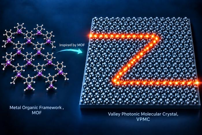
Inspired by Metal-Organic Framework based topological insulators, researchers at Tsinghua University proposed valley photonic molecular crystal (VPMC) and investigated the impact of molecular rotation on the valley-topological properties of VPMC. Credit: Tsinghua University/Xue Feng A research team led by Yidong Huang at Tsinghua University, including Xue Feng and Yongzhuo Li, has developed valley photonic molecular crystals (VPMCs) on a silicon platform. Combining theoretical modeling,...
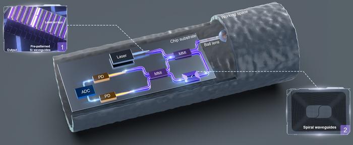
The system integrates a III-V semiconductor light source, SiN-based interferometers, Si-Ge photodetectors (PDs), and an integrated ball-lens microprobe, thereby combining the distinct advantages of multiple photonic integration platforms. The insets illustrate complementary technologies that can be incorporated to realize a miniaturized, fully integrated OCT system. Abbreviations: ADC, analog-to-digital converter. Inset 1: Foundry-scalable embedded III-V lasers on silicon-on-insulator (SOI)...

From left to right: Three photons with different quantum states enter an interferometer with three beam splitters. At each beam splitter, they can take different paths at the same time in superposition. The researchers then measured how often the three photons ended up together at the same output. Counterintuitively, it is possible to make the photons more similar to each other and at the same make them less likely to “bunch” together. AI-generated illustration, by Leonardo Novo. We usually...
