Columbia University

Researchers at Columbia University and University of California, San Diego, have introduced a novel "multi-messenger" approach to quantum physics that signifies a technological leap in how scientists can explore quantum materials.
The findings appear in a recent article published in Nature Materials, led by A. S. McLeod, postdoctoral researcher, Columbia Nano Initiative, with co-authors Dmitri Basov and A. J. Millis at Columbia and R.A. Averitt at UC San Diego.
"We have brought a technique from the inter-galactic scale down to the realm of the ultra-small," said Basov, Higgins Professor of Physics and Director of the Energy Frontier Research Center at Columbia. Equipped with multi-modal nanoscience tools we can now routinely go places no one thought would be possible as recently as five years ago."
The work was inspired by "multi-messenger" astrophysics, which emerged during the last decade as a revolutionary technique for the study of distant phenomena like black hole mergers. Simultaneous measurements from instruments, including infrared, optical, X-ray and gravitational-wave telescopes can, taken together, deliver a physical picture greater than the sum of their individual parts.
The search is on for new materials that can supplement the current reliance on electronic semiconductors. Control over material properties using light can offer improved functionality, speed, flexibility and energy efficiency for next-generation computing platforms.
Experimental papers on quantum materials have typically reported results obtained by using only one type of spectroscopy. The researchers have shown the power of using a combination of measurement techniques to simultaneously examine electrical and optical properties.
The researchers performed their experiment by focusing laser light onto the sharp tip of a needle probe coated with magnetic material. When thin films of metal oxide are subject to a unique strain, ultra-fast light pulses can trigger the material to switch into an unexplored phase of nanometer-scale domains, and the change is reversible.
By scanning the probe over the surface of their thin film sample, the researchers were able to trigger the change locally and simultaneously manipulate and record the electrical, magnetic and optical properties of these light-triggered domains with nanometer-scale precision.
The study reveals how unanticipated properties can emerge in long-studied quantum materials at ultra-small scales when scientists tune them by strain.
"It is relatively common to study these nano-phase materials with scanning probes. But this is the first time an optical nano-probe has been combined with simultaneous magnetic nano-imaging, and all at the very low temperatures where quantum materials show their merits," McLeod said. "Now, investigation of quantum materials by multi-modal nanoscience offers a means to close the loop on programs to engineer them."
Multi-messenger nanoprobes of hidden magnetism in a strained manganite
A. S. McLeod, Jingdi Zhang, M. Q. Gu, F. Jin, G. Zhang, K. W. Post, X. G. Zhao, A. J. Millis, W. B. Wu, J. M. Rondinelli, R. D. Averitt & D. N. Basov
Nature Materials (2019)
DOI: 10.1038/s41563-019-0533-y
Contact information:
Dmitri N. Basov
Columbia Professor of Physics and director of the Energy Frontier Research Center
db3056@columbia.edu
Phone: (212) 853 1320
Basov group @ Columbia
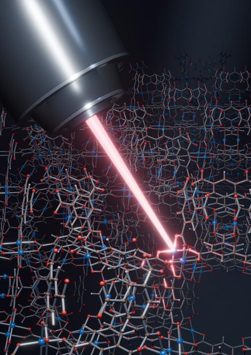
Filling the pores of a copper-based metal-organic framework with imidazolium ionic liquids makes the fragile material hard enough to pattern at room temperature. Treated Cu3BTC2 resisted the crystal damage seen in untreated samples during focused gallium ion beam etching, and researchers produced lines just 130 to 300 nanometres wide. The liquids appear to absorb heat and dissipate charge, and also raised hardness and thermal stability.
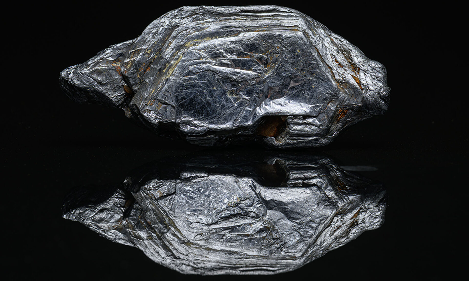
Engineers at the University of Rochester and Technion found that pressing a diamond nanoindenter tip a few nanometers into molybdenum can recrystallize the heat-resistant metal at room temperature, a process normally requiring about 1,000 degrees Celsius. Stopping the test just after the pop-in event reforms crystal grains in a tiny region around the dent, offering a way to repair defects and tailor properties locally.
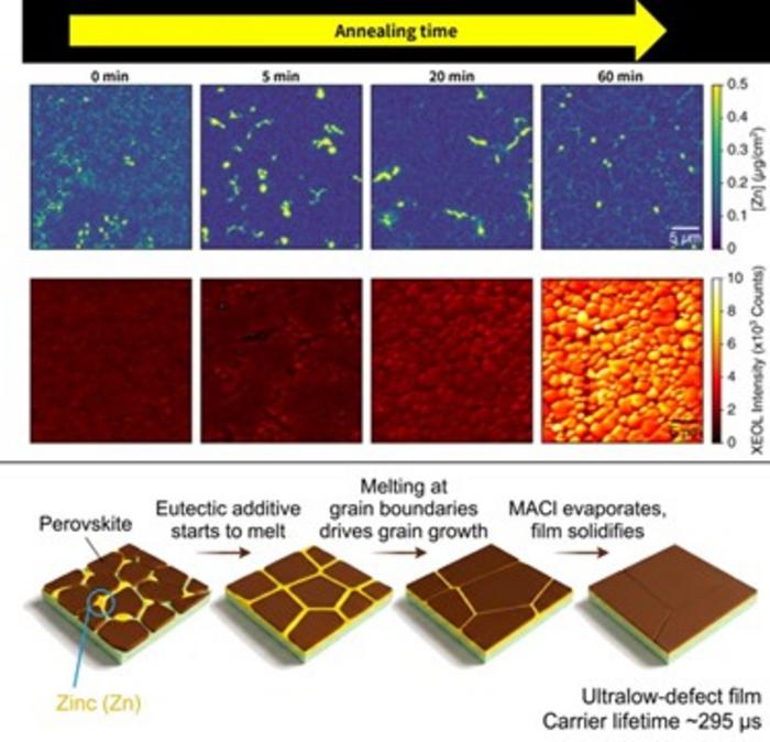
A eutectic mixture of methylammonium chloride and a zinc halide melts at about 100 degrees Celsius, forming a transient liquid layer at perovskite grain boundaries that lets crystals merge into larger, cleaner grains. The resulting films reached a carrier lifetime of roughly 295 microseconds and a surface recombination velocity of 0.3 cm/s, the lowest reported for lead halide perovskites.
This week in nanotech
9 deals tracked
New products
 Ti-WCMBN Nanomaterialia Featured
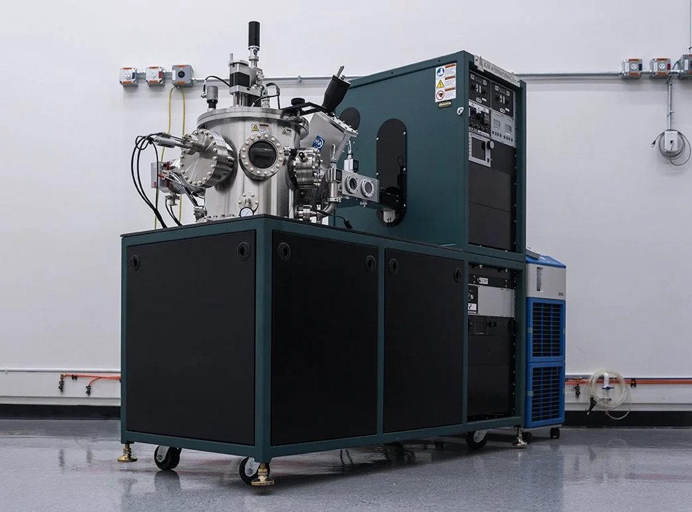 Orion Sputtering Deposition SystemsAJA International Featured
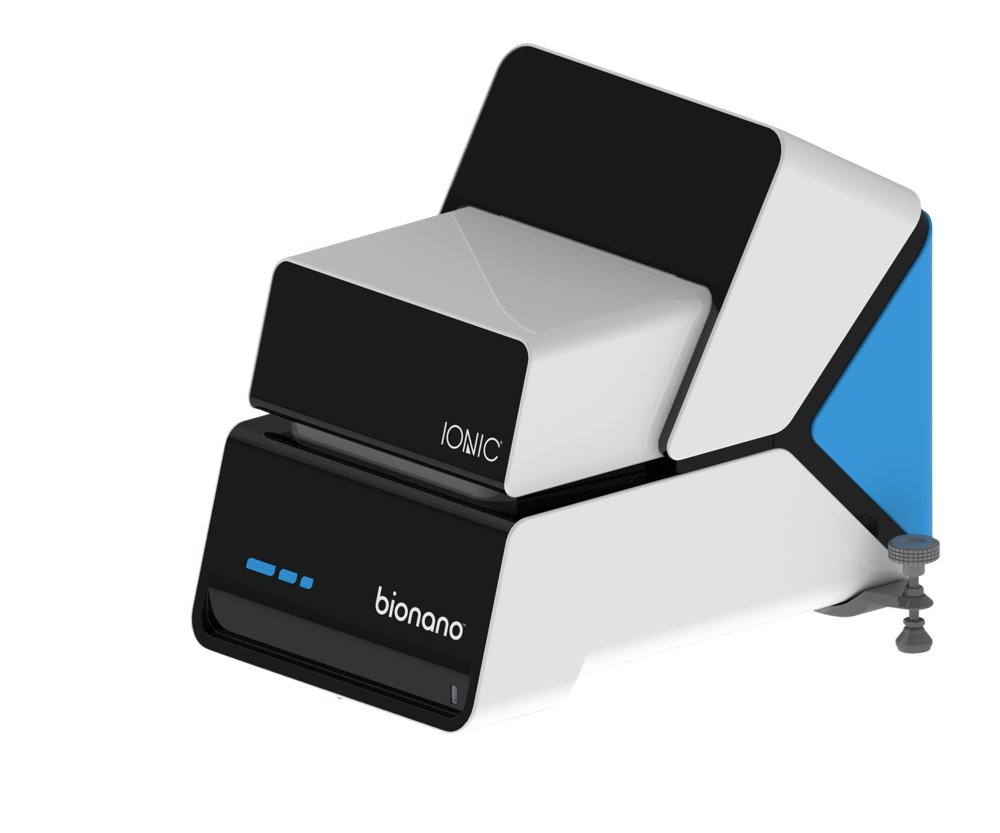 Ionic® Purification SystemBionano Genomics, Inc.
Market insights
Last 30 days: Semiconductors & Electronics was the busiest vertical: 39 of 130 events (30%).
Money raised per month