Leibniz Institute of Photonic Technology
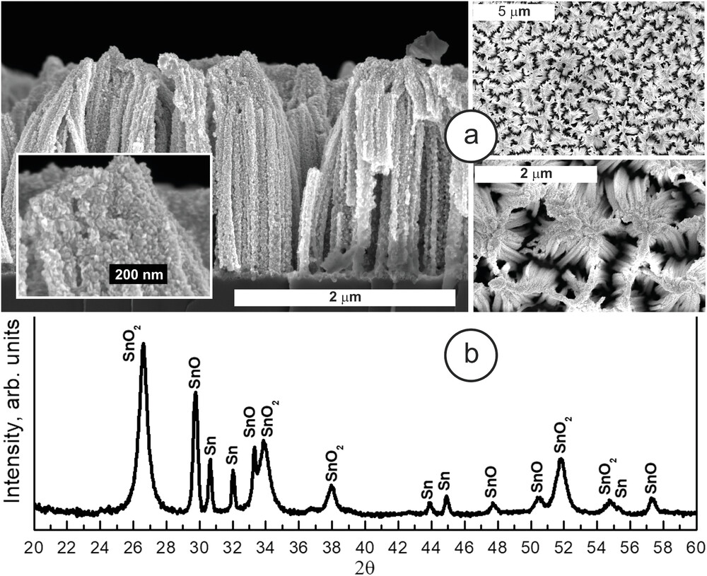
Nanometer-scale coatings with functional materials play an important role in many sensory, electronic and photonic applications. An international team of researchers – coordinated by Leibniz IPHT in Jena, Germany – has succeeded for the first time in observing novel growth effects of tin coatings on silicon nanometer-structured surfaces. With the knowledge gained, the chemical composition of deposited thin films can be precisely controlled and monitored in the future, opening up new applications in the fields of biophotonics, energy generation or mobility. The results were published in the journal Small.
Tin-containing layers are in demand for a wide variety of electronic parts and components in the electrical industry as well as in sensor technology or photovoltaics. Researchers from the Leibniz Institute of Photonic Technology (Leibniz IPHT) investigated the development process of nanoscale tin layers together with scientists from Germany, Russia and Great Britain and summarized their results in the renowned journal Small.
The starting material for the observed growth processes of tin-containing thin films are ultra-thin silicon-based structures in the form of nanowires with a diameter of less than 100 nanometers. In experimental studies, the researchers were able to demonstrate for the first time a specific distribution effect of tin along these silicon nanostructures: Tin-containing layers with different degrees of oxidation were formed along the entire length of the semiconductor nanowires by means of metal-organic chemical vapour deposition at a deposition temperature of 600 degrees Celsius.
"By understanding how tin coatings grow and which factors influence this growth process, we create the conditions for specifically controlling coating processes. This allows surfaces to be refined very precisely and to be equipped with desired functional properties at previously defined positions," explains Dr. Vladimir Sivakov, head of the Silicon Nanostructures Group at Leibniz IPHT, who investigated and discovered the growth mechanisms together with his team.
Applications of ultra-thin tin layers
Nanometer-thin coatings with tin enable specific optical and electrical properties and allow, among other things, to further improve the research and development of optical and biophotonic methods. Tin layers can be used as UV-SERS-active surfaces in surface-enhanced Raman scattering (SERS) spectroscopy, which can be applied to determine the molecular fingerprint of biological samples using SERS-active metal nanostructures. In addition, there are areas of application in gas sensors in which tin reacts to gases as a highly sensitive layer. Application scenarios in high-performance lithium-ion batteries for electromobility and thermal energy storage are also conceivable, in which tin-coated anodes ensure high electronic conductivity.
Mechanisms and growth dynamics of tin-containing layers
The researchers investigated the growth dynamics of the observed tin-based layers on nanostructured surfaces using microscopic and spectroscopic methods. In contrast to planar and unstructured silicon surfaces, on which the deposition took place homogeneously, the surfaces of the semiconductor nanowires were covered with tin-containing crystals of different sizes and shapes over the entire length.
The results presented in the journal Small show the formation of different tin oxide phases along the nanostructured silicon surfaces, which could be identified with tin dioxide (SnO2) in the upper part, tin monoxide (SnO) in the middle part and with metallic tin (Sn) in the lower part.
The amount and distribution of the formed metallic Sn and its SnO and SnO2 oxides can be explained and effectively controlled by the length, diameter, porosity, and spacing of the silicon-based semiconductor nanostructures. In addition to these geometrical parameters, the researchers were able to reveal the formation of hydrocarbon-containing by-products as reducing agents for tin oxide reduction as another factor influencing the distribution of the formed tin layers along the semiconductor nanostructures. The thermal conductivity of the silicon structures and thus the temperature distribution along the nanowires during the high-temperature vapour deposition can also have an influence on the formation of different tin oxide phases.
References
Nanostructured Silicon Matrix for Materials Engineering
Poting Liu, Alexander Schleusener, Gabriel Zieger, Arne Bochmann, Matthijs A. van Spronsen, Vladimir Sivakov
https://onlinelibrary.wiley.com/doi/10.1002/smll.202206318
Spectromicroscopy Studies of Silicon Nanowires Array Covered by Tin Oxide Layers
Sergey Turishchev, Alexander Schleusener, Olga Chuvenkova, Elena Parinova, Poting Liu, Maxim Manyakin, Sergei Kurganskii, Vladimir Sivakov

Waste polyamide-derived CQDs show continuous photoluminescence tuning from 308 to 552 nm through sequential defect-state engineering, with optical transition energies decreasing from 4.32 to 2.50 eV. @Christian Ebere Enyoh from Saitama University Carbon quantum dots (CQDs) are fluorescent carbon nanomaterials with potential applications in sensing, optoelectronics, displays, anti-counterfeiting, and environmental technologies. Their optical properties can be adjusted by modifying the carbon...

The researchers used circularly polarized light at normal incidence and found that helicity-dependent photocurrents appeared perpendicular to the crystal’s polarization but vanished when measured parallel to it, supporting a bulk origin of CPGE. @Institute of Science Tokyo The circular photogalvanic effect (CPGE), a phenomenon that generates helicity-dependent photocurrents in noncentrosymmetric materials, can originate purely from a crystal's internal structure without contribution from the...

Summary of gold nanoparticle growth programming in liposome based on localization of biomineralization peptide The position of biomineralization peptides within liposomes can influence how gold nanoparticles grow, reports a research team from Institute of Science Tokyo. Peptides localized at the membrane interface promote branched structures, while those confined to the liposome interior favor spherical nanoparticles. The findings offer a new strategy for controlling nanoscale reaction...
