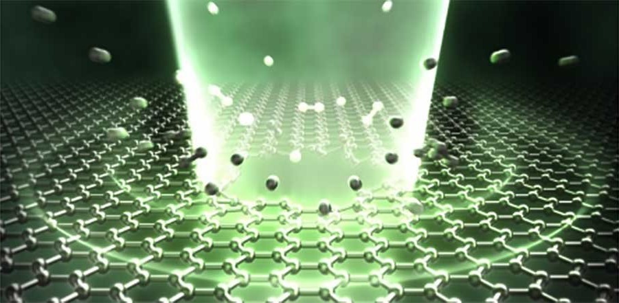
Discovered in 2004, graphene has revolutionized various scientific fields. It possesses remarkable properties like high electron mobility, mechanical strength, and thermal conductivity. Extensive time and effort have been invested in exploring its potential as a next-generation semiconductor material, leading to the development of graphene-based transistors, transparent electrodes, and sensors.
But to render these devices into practical application, it's crucial to have efficient processing techniques that can structure graphene films at micrometer and nanometer scale. Typically, micro/nanoscale material processing and device manufacturing employ nanolithography and focused ion beam methods. However, these have posed longstanding challenges for laboratory researchers due to their need for large-scale equipment, lengthy manufacturing times, and complex operations.
Back in January, Tohoku University researchers created a technique that could micro/nanofabricate silicon nitride thin devices with thicknesses ranging from 5 to 50 nanometers. The method employed a femtosecond laser, which emitted extremely short, rapid pulses of light. It turned out to be capable of quickly and conveniently processing thin materials without a vacuum environment.
By applying this method to an ultra-thin atomic layer of graphene, the same group has now succeeded in performing a multi-point hole drilling without damaging the graphene film. Details of their breakthrough were reported in the journal Nano Letters on May 16, 2023.
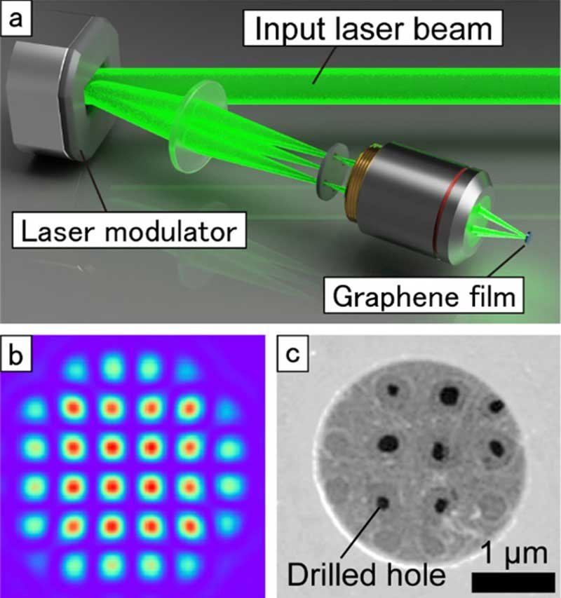
"With proper control of the input energy and number of laser shots, we were able to execute precise machining and create holes with diameters ranging from 70 nanometers - much smaller than the laser wavelength of 520 nanometers - to over 1 millimeter," says Yuuki Uesugi, assistant professor at Tohoku University's Institute of Multidisciplinary Research for Advanced Materials, and co-author of the paper.
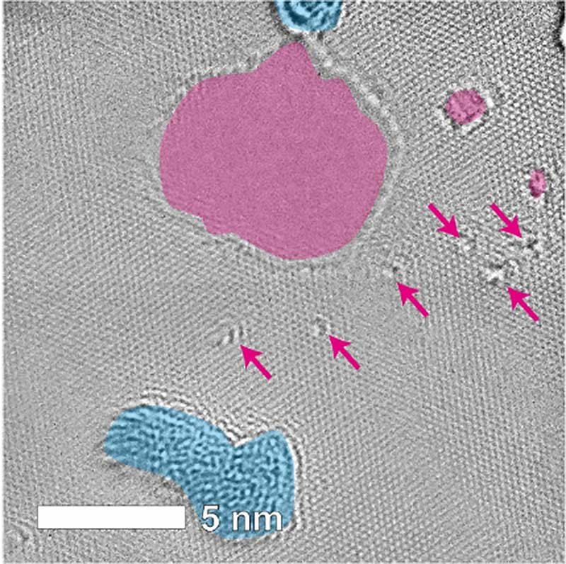
Upon closer examination of the areas irradiated with low-energy laser pulses, which did not make holes, via a high-performance electron microscope, Uesugi and his colleagues found that contaminants on the graphene had also been removed. Further magnified observation revealed nanopores less than 10 nanometers in diameter and atomic-level defects, where several carbon atoms were missing in the crystal structures of the graphene.
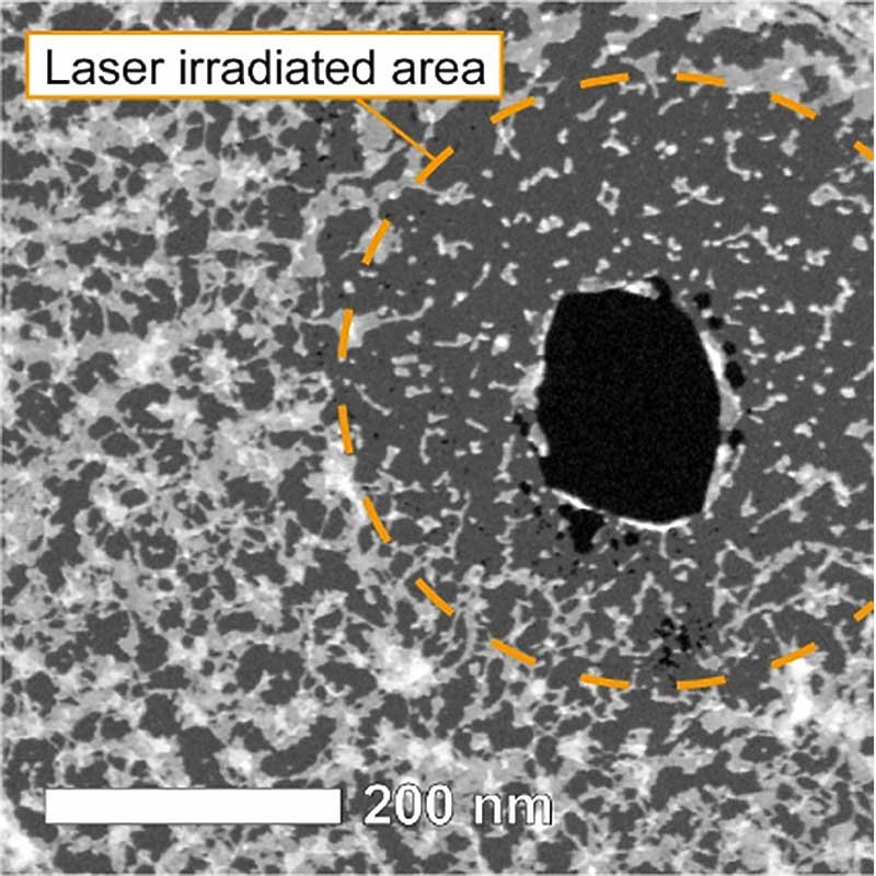
Atomic defects in graphene are both detrimental and advantageous, depending on the application. Whilst defects sometimes downgrade certain properties, they also introduce new functionalities or enhance specific characteristics.
"Observing a tendency for the density of nanopores and defects to increase proportionally with the energy and number of laser shots led us to conclude the formation of nanopores and defects could be manipulated by using a femtosecond laser irradiation," adds Uesugi. "By forming nanopores and atomic-level defects in graphene, not only can electrical conductivity be controlled but also quantum-level characteristics such as spin and valley. Moreover, the contaminant removal by femtosecond laser irradiation found in this research could develop a new method for non-destructively and cleanly washing high-purity graphene."
Looking ahead, the team aims to establish a cleaning technique using the laser and carry a detailed investigation into how to conduct atomic defect formation. Further breakthroughs will have a big impact on areas from quantum materials research to biosensor development.
Reference
Nanoprocessing of Self-Suspended Monolayer Graphene and Defect Formation by Femtosecond-Laser Irradiation
Naohiro Kadoguchi, Yuuki Uesugi, Makoto Nagasako, Tetsuro Kobayashi, Yuichi Kozawa, and Shunichi Sato

Waste polyamide-derived CQDs show continuous photoluminescence tuning from 308 to 552 nm through sequential defect-state engineering, with optical transition energies decreasing from 4.32 to 2.50 eV. @Christian Ebere Enyoh from Saitama University Carbon quantum dots (CQDs) are fluorescent carbon nanomaterials with potential applications in sensing, optoelectronics, displays, anti-counterfeiting, and environmental technologies. Their optical properties can be adjusted by modifying the carbon...

The researchers used circularly polarized light at normal incidence and found that helicity-dependent photocurrents appeared perpendicular to the crystal’s polarization but vanished when measured parallel to it, supporting a bulk origin of CPGE. @Institute of Science Tokyo The circular photogalvanic effect (CPGE), a phenomenon that generates helicity-dependent photocurrents in noncentrosymmetric materials, can originate purely from a crystal's internal structure without contribution from the...

Summary of gold nanoparticle growth programming in liposome based on localization of biomineralization peptide The position of biomineralization peptides within liposomes can influence how gold nanoparticles grow, reports a research team from Institute of Science Tokyo. Peptides localized at the membrane interface promote branched structures, while those confined to the liposome interior favor spherical nanoparticles. The findings offer a new strategy for controlling nanoscale reaction...
