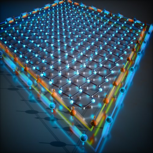
Researchers from the University of Twente proved that germanene, a two-dimensional material made of germanium atoms, behaves as a topological insulator. It is the first 2D topological insulator that consists of a single element. It also has the unique ability to switch between ‘on’ and ‘off’ states, comparable to transistors. This could lead to more energy-efficient electronics.
Topological insulators are materials with the unique property of insulating electricity in their interior while conducting electricity along their edges. The conductive edges allow electrical current to flow without energy loss. “At the moment, electronic devices lose a lot of energy in the form of heat, because defects in the material increase the resistance. As a result, your mobile phone can get uncomfortably hot”, explains UT researcher Pantelis Bampoulis. While scattering at defects is allowed in normal materials, at the edges of 2D topological insulators, the scattering of electrons at defects is forbidden due to the unique topological protection mechanism. Therefore, electrical current in 2D topological insulators flows without dissipating energy. This makes them more energy-efficient than current electronic materials.
Creating germanene
Germanene is such a 2D topological insulator. “Current topological insulators consist of complex structures from different types of elements. Germanene is unique in that it’s made from just a single element”, explains Bampoulis. To create this exciting material, the researchers melted germanium together with platinum. When the mixture cooled down, a tiny layer of germanium atoms arranged into a honeycomb lattice on top of the germanium-platinum alloy. This 2D layer of atoms is called germanene.
Topological transistors
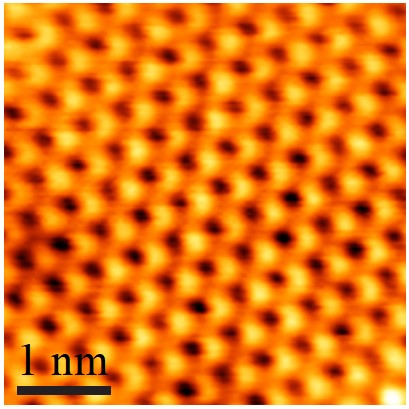
The researchers also discovered that the conducting properties of the material can be switched ‘off’ by applying an electric field. This property is unique for a topological insulator. “The possibility to switch between ‘on’ and ‘off’ states adds an exciting application case for germanene”, says Bampoulis. It paves the way for designing topological field-effect transistors. These transistors could replace traditional transistors in electronic devices. Resulting in electronics that no longer heat up.
Reference
Quantum Spin Hall States and Topological Phase Transition in Germanene
Pantelis Bampoulis, Carolien Castenmiller, Dennis J. Klaassen, Jelle van Mil, Yichen Liu, Cheng-Cheng Liu, Yugui Yao, Motohiko Ezawa, Alexander N. Rudenko, and Harold J. W. Zandvliet
https://journals.aps.org/prl/abstract/10.1103/PhysRevLett.130.196401

Waste polyamide-derived CQDs show continuous photoluminescence tuning from 308 to 552 nm through sequential defect-state engineering, with optical transition energies decreasing from 4.32 to 2.50 eV. @Christian Ebere Enyoh from Saitama University Carbon quantum dots (CQDs) are fluorescent carbon nanomaterials with potential applications in sensing, optoelectronics, displays, anti-counterfeiting, and environmental technologies. Their optical properties can be adjusted by modifying the carbon...

The researchers used circularly polarized light at normal incidence and found that helicity-dependent photocurrents appeared perpendicular to the crystal’s polarization but vanished when measured parallel to it, supporting a bulk origin of CPGE. @Institute of Science Tokyo The circular photogalvanic effect (CPGE), a phenomenon that generates helicity-dependent photocurrents in noncentrosymmetric materials, can originate purely from a crystal's internal structure without contribution from the...

Summary of gold nanoparticle growth programming in liposome based on localization of biomineralization peptide The position of biomineralization peptides within liposomes can influence how gold nanoparticles grow, reports a research team from Institute of Science Tokyo. Peptides localized at the membrane interface promote branched structures, while those confined to the liposome interior favor spherical nanoparticles. The findings offer a new strategy for controlling nanoscale reaction...
