National Institute of Standards and Technology
Atoms are notoriously difficult to control. They zigzag like fireflies, tunnel out of the strongest containers and jitter even at temperatures near absolute zero.
Nonetheless, scientists need to trap and manipulate single atoms in order for quantum devices, such as atomic clocks or quantum computers, to operate properly. If individual atoms can be corralled and controlled in large arrays, they can serve as quantum bits, or qubits — tiny discrete units of information whose state or orientation may eventually be used to carry out calculations at speeds far greater than the fastest supercomputer.
Researchers at the National Institute of Standards and Technology (NIST), together with collaborators from JILA — a joint institute of the University of Colorado and NIST in Boulder — have for the first time demonstrated that they can trap single atoms using a novel miniaturized version of “optical tweezers” — a system that grabs atoms using a laser beam as chopsticks.
Ordinarily, optical tweezers, which garnered the 2018 Nobel Prize in Physics, feature bulky centimeter-size lenses or microscope objectives outside the vacuum holding individual atoms. NIST and JILA have previously used the technique with great success to create an atomic clock.
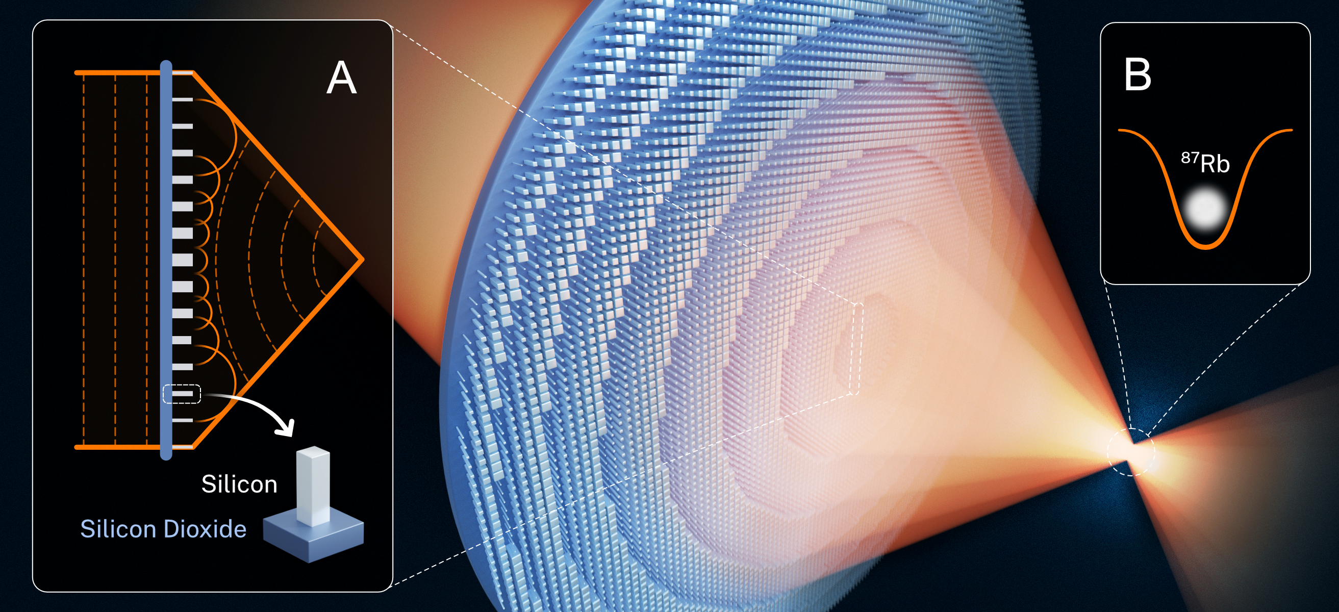
In the new design, instead of typical lenses, the NIST team used unconventional optics — a square glass wafer about 4 millimeters in length imprinted with millions of pillars only a few hundreds of nanometers (billionths of a meter) in height that collectively act as tiny lenses. These imprinted surfaces, dubbed metasurfaces, focus laser light to trap, manipulate and image individual atoms within a vapor. The metasurfaces can operate in the vacuum where the cloud of trapped atoms is located, unlike ordinary optical tweezers.
The process involves several steps. First, incoming light that has a particularly simple form, known as a plane wave, strikes groups of the tiny nanopillars. (Plane waves are like moving parallel sheets of light that have a uniform wavefront, or phase, whose oscillations remain in sync with each other and neither diverge nor converge as they travel.) The groupings of nanopillars transform the plane waves into a series of little wavelets, each of which is slightly out of sync with its neighbor. As a result, adjacent wavelets reach their peak at slightly different times.
These wavelets combine or “interfere” with each other, causing them to focus all their energy at a specific position — the location of the atom that is to be trapped.
Depending on the angle at which the incoming plane waves of light strike the nanopillars, the wavelets are focused at slightly different places, enabling the optical system to trap a series of individual atoms that reside at slightly different locations from each other.
Because the mini flat-lenses can be operated within a vacuum chamber and require no moving parts, the atoms can be trapped without having to build and manipulate a complex optical system, said NIST researcher Amit Agrawal. Other researchers at NIST and JILA have previously used conventional optical tweezers with great success to design atomic clocks.
In the new study, Agrawal and two other NIST scientists, Scott Papp and Wenqi Zhu, along with collaborators from Cindy Regal’s group at JILA, designed, fabricated and tested the metasurfaces and performed single-atom trapping experiments.
In a paper published today in PRX Quantum, the researchers reported that they had separately trapped nine single rubidium atoms. The same technique, scaled up by using multiple metasurfaces or one with large field of view, should be able to confine hundreds of single atoms, Agrawal said, and could lead the way to routinely trap an array of atoms using a chip-scale optical system.
The system held the atoms in place for about 10 seconds, which is long enough to study the quantum mechanical properties of the particles and use them to store quantum information. (Quantum experiments operate on time scales of ten millionths to thousandths of a second.)
To demonstrate that they captured the rubidium atoms, the researchers illuminated them with a separate light source, causing them to fluoresce. The metasurfaces then played a second critical role. Initially, they had shaped and focused the incoming light that trapped the rubidium atoms. Now the metasurfaces captured and focused the fluorescent light emitted by these same atoms, redirecting the fluorescent radiation into a camera in order to image the atoms.
The metasurfaces can do more than just confine single atoms. By focusing light with pinpoint accuracy, the metasurfaces can coax individual atoms into special quantum states, tailored for specific atom-trapping experiments.
For example, polarized light directed by the tiny lenses can cause an atom’s spin — a quantum attribute analogous to the Earth spinning on its axis — to point in a particular direction. These interactions between focused light and single atoms are useful for many types of atom-scale experiments and devices, including future quantum computers.
Reference
Single-Atom Trapping in a Metasurface-Lens Optical Tweezer
T.-W. Hsu, W. Zhu, T. Thiele, M. O. Brown, S. B. Papp, A. Agrawal, and C. A. Regal
https://journals.aps.org/prxquantum/abstract/10.1103/PRXQuantum.3.030316

A Fourier transform revealing spatial patterns on the surface at 300 millikelvins. A charge density wave signals the presence of the pair density wave. The background is tellurium atoms on the surface of uranium ditelluride. @University of Illinois Urbana-Champaign’s Grainger College of Engineering Physicists with the University of Illinois Urbana-Champaign’s Grainger College of Engineering have identified a new form of superconducting behavior. Experiments on the metal uranium ditelluride...
Stack two atomically thin layers, rotate one slightly against the other, and a new material emerges. The resulting moiré pattern can slow electrons down so much that their interactions take over. This produces superconductivity, magnetism and exotic fractional quantum states that neither layer shows on its own. This field, known as twistronics, has become one of the most active frontiers in condensed matter physics. So far, however, it has been built on only a handful of materials, mainly...

From a two-colour diffraction pattern (left), two snapshots of a helium droplet doped with xenon nanoparticles can be reconstructed (centre). These images can inform a potential 3D rendering of a xenon-doped helium nanodroplet (right). An overarching goal of ultrafast science is to enable researchers to watch structural changes in matter on their natural timescale. Experimentally, this translates into taking two snapshots of the same nanoscale object that are only femtoseconds apart to...
