Semiconductor advancement could lead to low-cost, flexible electronic devices
- May 24, 2024
- 2 min read
The public’s appetite for inexpensive and powerful electronic devices continues to grow.
While silicon-based semiconductors have been key to satiating this demand, a superior alternative could be wide-bandgap semiconductors. These materials, which operate at higher temperatures and handle increased power loads, are unfortunately very expensive.
An innovation, described in a study published May 2 in Scientific Reports, could help change that. The work was led by researchers at the University at Buffalo, Texas State University and TapeSolar Inc.
The study centers on a fabrication technique called epitaxial deposition, which involves precisely placing molecules on top of a crystal substrate so that they match perfectly.
In conventional semiconductors, machines deposit thin films of gallium arsenide epitaxially on single-crystal gallium arsenide substrates. (These single-crystal gallium arsenide films have unique physical and electrical properties which are ideal for fabrication of high-performance semiconductor devices used in solar panels and many other electronic devices.)
In addition to being expensive, gallium arsenide substrates are only available in small sizes and are rigid – meaning they cannot conform to curved surfaces. Alternative fabrication methods – such as epitaxial lift-off and direct wafer bonding – are promising but yet to be proven successful.
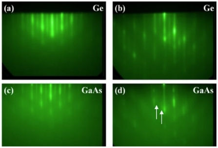
In the new study, the researchers used epitaxial deposition. However, instead of single crystal substrates, they employed a single-crystal-like germanium substrate that is flexible and can be fabricated using roll-to-roll manufacturing. This process – similar to a printing press – is cost-effective and efficient.
(In 2022, the same team reported on creating single-crystal-like germanium substrates in PNAS Nexus, the open access sibling journal of the Proceedings of the National Academy of Sciences.)
Researchers analyzed the new gallium arsenide semiconductor through X-ray diffraction, electron microscopy and photoluminescence spectrometry.
“These single-crystal-like, gallium arsenide films could potentially be useful in numerous applications where large areas, flexibility, light weight and high performance are of interest,” says the study’s corresponding author Amit Goyal, PhD, SUNY Distinguished Professor and SUNY Empire Innovation Professor in the Department of Chemical and Biological Engineering in UB School of Engineering and Applied Sciences. Reference Heteroepitaxial GaAs thin-films on flexible, large-area, single-crystal-like substrates for wide-ranging optoelectronic applications
Gokul Radhakrishnan, Kyunghoon Kim, Ravi Droopad & Amit Goyal


Comments