DOE/Ames Laboratory
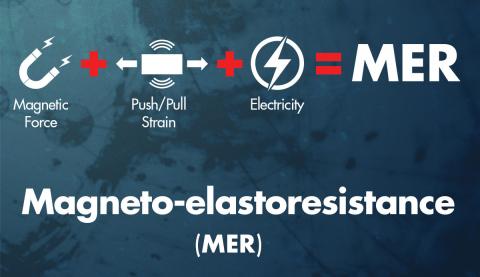
Experimental physicists have combined several measurements of quantum materials into one in their ongoing quest to learn more about manipulating and controlling the behavior of them for possible applications. They even coined a term for it-- Magneto-elastoresistance, or MER.
Scientists in condensed matter physics at the U.S. Department of Energy's Ames Laboratory have a long history of investigating "weird" materials, according to Paul Canfield, Ames Lab physicist, Distinguished Professor and the Robert Allen Wright Professor of Physics and Astronomy at Iowa State University.
"Weird" in this case means metallic and semi-metallic compounds that have magnetic, superconducting, or other properties that might be useful in tech applications such as quantum computing. To force those compounds to reveal their secrets, however, experimentalists must poke, prod, and measure the materials to see how and how much they react.
Canfield and his fellow researchers systematically studied WTe2, a semi-metal, by exposing it to electric current, magnetic field, and strain from pushing and pulling. The measurements of resistance under a combination of external magnetic field and strain-- was something that had not been studied in any systematic matter before.
They found that the material reacted with large changes in elastoresistance and that it was further controllable by magnetic field, especially at low temperatures.
By pairing experimental findings with density functional theory and modeling, "we were able to demonstrate that MER is tied to the redistribution of carriers from different bands (i.e. heavy hole band, light hole and electron band)" said Na Hyun Jo, a postdoctoral research associate at Ames Laboratory. "This means engineering WTe2 and others like it is possible for future applications."
Scientist Sergey Bud'ko was gratified by the outcome of the experiment, showing a large effect in MER, proving to the larger scientific community that it's a worthy way of looking for similar effects in similar materials and learning how or when they will occur. "While we have investigated a number of these materials with large magnetoresistance over the decades, we are only just beginning to get a sense of why some materials demonstrate it and not others; here we open the door to a clearer theoretical explanation of their properties."
Magnetoelastoresistance in WTe2: Exploring electronic structure and extremely large magnetoresistance under strain
Na Hyun Jo, Lin-Lin Wang, Peter P. Orth, Sergey L. Bud’ko, and Paul C. Canfield
Proceedings of the National Academy of Sciences 2019 116 (51) 25524-25529
Contact information:
Paul Canfield
Ames Lab physicist & Iowa State University Professor of Physics and Astronomy
canfield@ameslab.gov / pcc@iastate.edu
Phone: 515-294-6270
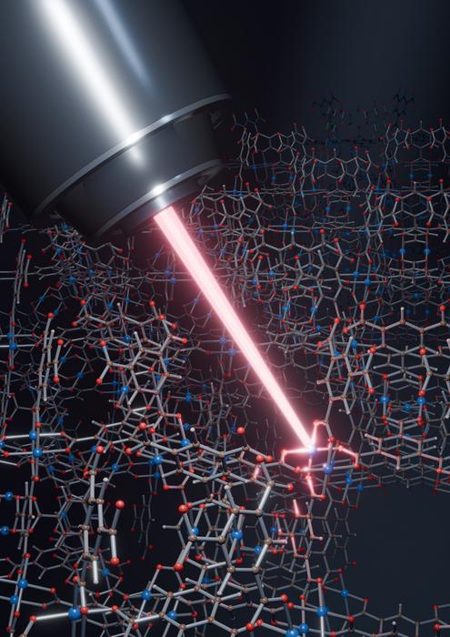
Filling the pores of a copper-based metal-organic framework with imidazolium ionic liquids makes the fragile material hard enough to pattern at room temperature. Treated Cu3BTC2 resisted the crystal damage seen in untreated samples during focused gallium ion beam etching, and researchers produced lines just 130 to 300 nanometres wide. The liquids appear to absorb heat and dissipate charge, and also raised hardness and thermal stability.
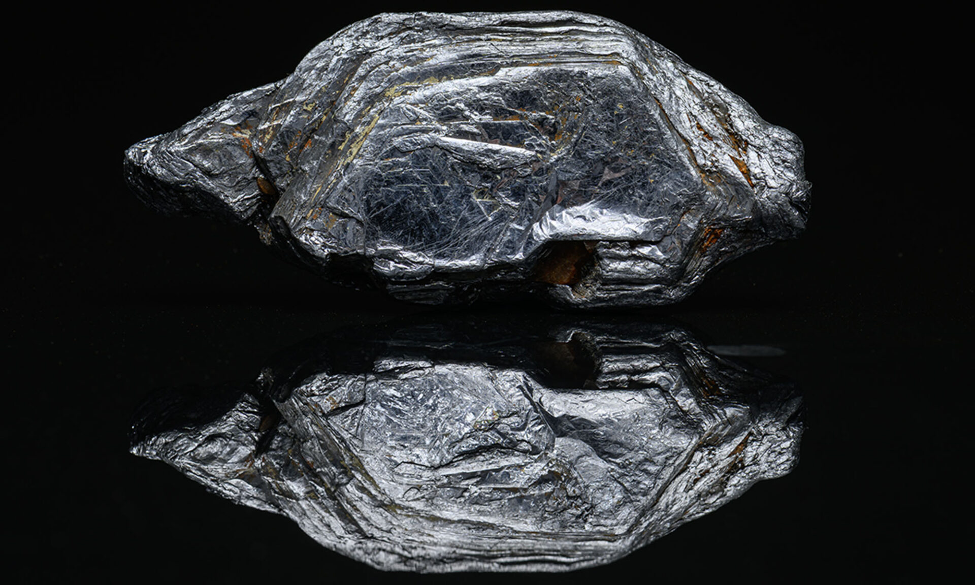
Engineers at the University of Rochester and Technion found that pressing a diamond nanoindenter tip a few nanometers into molybdenum can recrystallize the heat-resistant metal at room temperature, a process normally requiring about 1,000 degrees Celsius. Stopping the test just after the pop-in event reforms crystal grains in a tiny region around the dent, offering a way to repair defects and tailor properties locally.
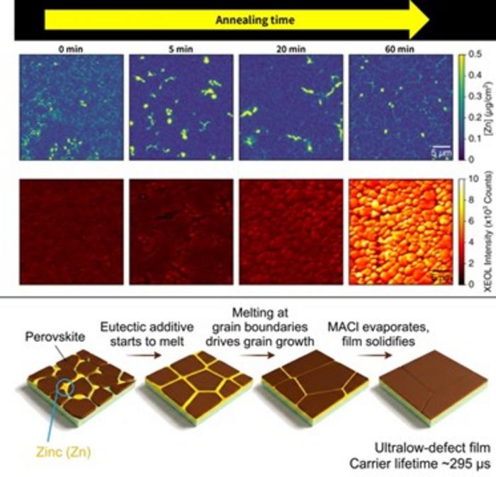
A eutectic mixture of methylammonium chloride and a zinc halide melts at about 100 degrees Celsius, forming a transient liquid layer at perovskite grain boundaries that lets crystals merge into larger, cleaner grains. The resulting films reached a carrier lifetime of roughly 295 microseconds and a surface recombination velocity of 0.3 cm/s, the lowest reported for lead halide perovskites.
This week in nanotech
9 deals tracked
New products
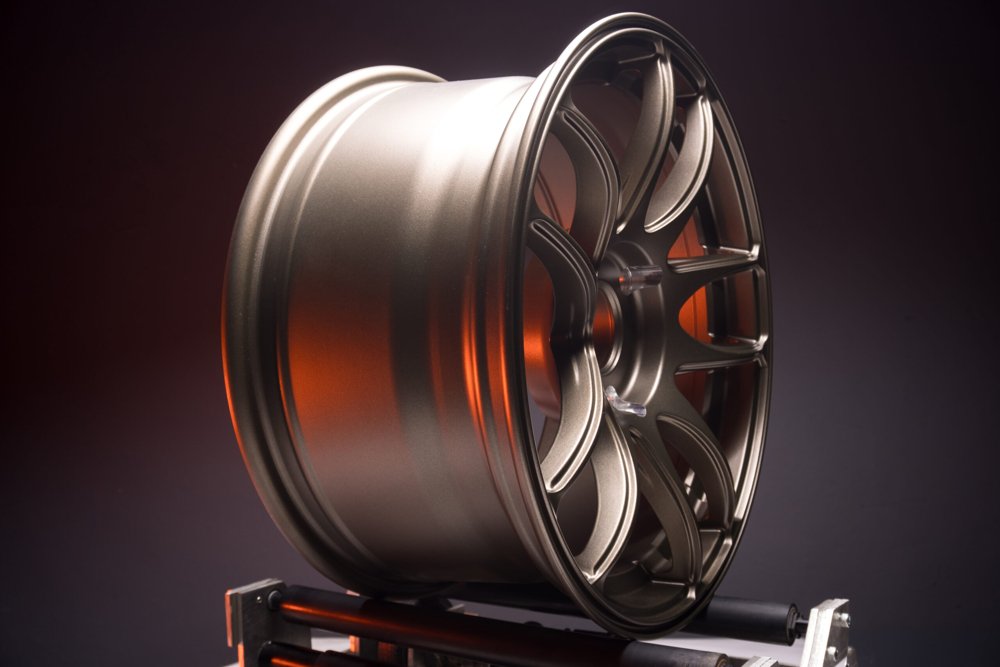 Ti-WCMBN Nanomaterialia Featured
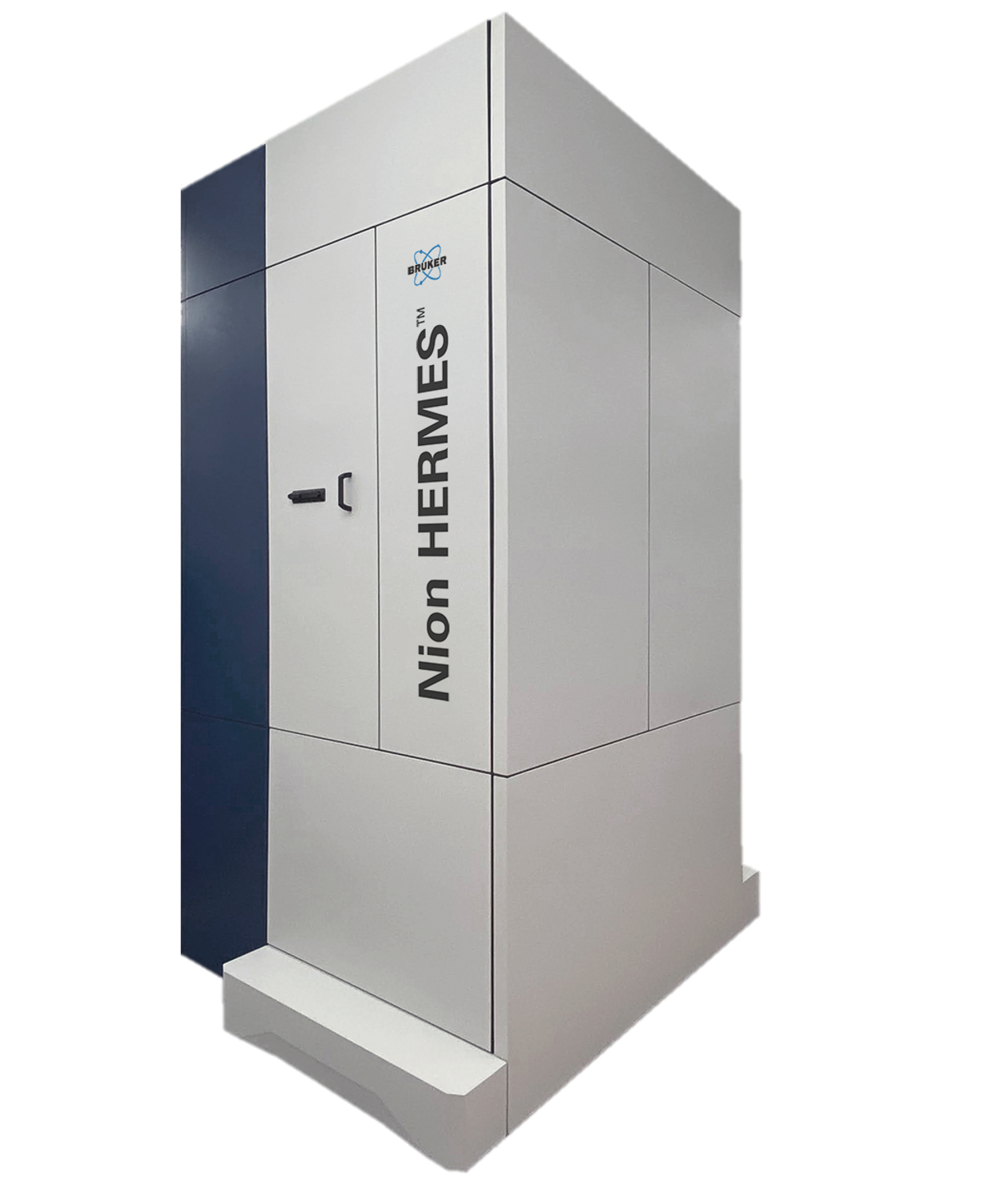 Nion-compatible In Situ STEM Holders for Electrical BiasingHummingbird Scientific Featured
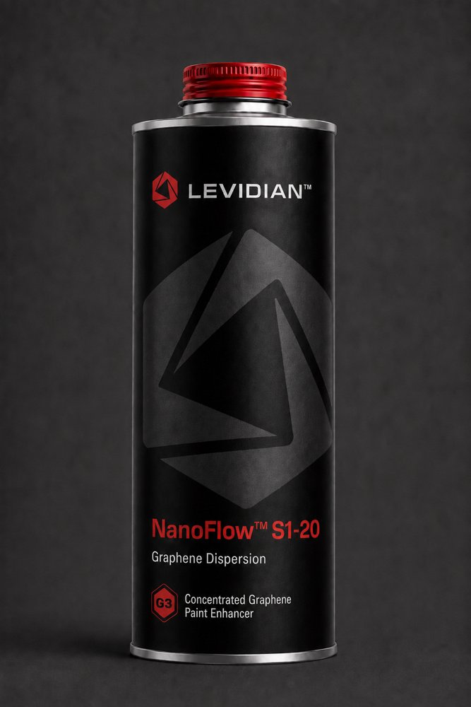 NanoFlow® S1-20Levidian
Market insights
Last 30 days: Semiconductors & Electronics was the busiest vertical: 39 of 130 events (30%).
Money raised per month