Filming the film: Scientists observe photographic exposure live at the nanoscale
- Jun 9, 2015
- 3 min read

Advanced method opens up new opportunities for investigation of dynamic processes
Photoinduced chemical reactions are responsible for many fundamental processes and technologies, from energy conversion in nature to micro fabrication by photo-lithography. One process that is known from everyday’s life and can be observed by the naked eye, is the exposure of photographic film. At DESY's X-ray light source PETRA III, scientists have now monitored the chemical processes during a photographic exposure at the level of individual nanoscale grains in real-time. The advanced experimental method enables the investigation of a broad variety of chemical and physical processes in materials with millisecond temporal resolution, ranging from phase transitions to crystal growth. The research team lead by Prof. Jianwei (John) Miao from the University of California in Los Angeles (UCLA) and Prof. Tim Salditt from the University of Göttingen report their technique and observations in the journal Nature Materials.
The researchers investigated a photographic paper (Kodak linagraph paper Type 2167or “yellow burn paper”) that is often used to determine the position of the beam at X-ray experiments. “The photographic paper we looked at is not specially designed for X-rays. It works by changing its colour on exposure to light or X-rays,” explains DESY physicist Dr. Michael Sprung, head of the PETRA III beamline P10 where the experiments took place.
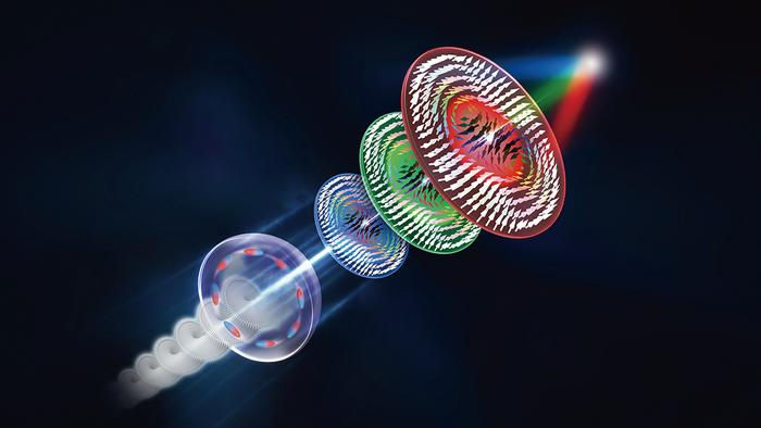
The X-rays were not only used to expose the photographic paper, but also to analyse changes of its inner composition at the same time. The paper carries a photosensitive film of a few micrometre thickness, consisting of tiny silver bromide grains dispersed in a gelatine matrix, and with an average size of about 700 nanometres. A nanometre is a millionth of a millimetre. When X-rays impinge onto such a crystalline grain, they are diffracted in a characteristic way, forming a unique pattern on the detector that reveals properties like crystal lattice spacing, chemical composition and orientation. “We could observe individual silver bromide grains within the ‘burn’ paper since the X-ray beam had a size of only 270 by 370 nanometres – smaller than the average grain,” says Salditt, who is a partner of DESY in the construction and operation of the GINIX (Göttingen Instrument for Nano-Imaging with X-Rays) at beamline P10.

The X-ray exposure starts the photolysis from silver bromide to produce silver. An absorbed X-ray photon can create many photolytic silver atoms, which grow and agglomerate at the surface and inside the silver bromide grain. The scientists observed how the silver bromide grains were strained, began to turn in the gelatine matrix and broke up into smaller crystallites as well as the growth of pure silver nano grains. The exceptionally bright beam of PETRA III together with a high-speed detector enabled the ‘filming’ of the process with up to five milliseconds temporal resolution. “We observed, for the first time, grain rotation and lattice deformation during photoinduced chemical reactions,” emphasises Miao. “We were actually surprised how fast some of these single grains rotate,” adds Sprung. “Some spin almost one time every two seconds.”
“As advanced synchrotron light sources are currently under rapid development in the US, Europe and Asia,” the authors anticipate that “in situ X-ray nanodiffraction, which enables to measure atomic resolution diffraction patterns with several millisecond temporal resolution, can be broadly applied to investigate phase transitions, chemical reactions, crystal growth, grain boundary dynamics, lattice expansion, and contraction in materials science, nanoscience, physics, and chemistry.”
Reference Grain rotation and lattice deformation during photoinduced chemical reactions revealed by in situ X-ray nanodiffraction; Zhifeng Huang, Matthias Bartels, Rui Xu, Markus Osterhoff, Sebastian Kalbfleisch, Michael Sprung, Akihiro Suzuki, Yukio Takahashi, Thomas N. Blanton, Tim Salditt und Jianwei Miao; Nature Materials, 2015; DOI: 10.1038/NMAT4311


Comments