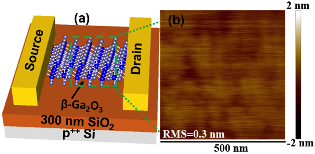
Researchers have demonstrated the high-performance potential of an experimental transistor made of a semiconductor called beta gallium oxide, which could bring new ultra-efficient switches for applications such as the power grid, military ships and aircraft.
The semiconductor is promising for next-generation “power electronics,” or devices needed to control the flow of electrical energy in circuits. Such a technology could help to reduce global energy use and greenhouse gas emissions by replacing less efficient and bulky power electronics switches now in use.
The transistor, called a gallium oxide on insulator field effect transistor, or GOOI, is especially promising because it possesses an “ultra-wide bandgap,” a trait needed for switches in high-voltage applications.
Compared to other semiconductors thought to be promising for the transistors, devices made from beta gallium oxide have a higher “breakdown voltage,” or the voltage at which the device fails, said Peide Ye, Purdue University's Richard J. and Mary Jo Schwartz Professor of Electrical and Computer Engineering.
Findings are detailed in a research paper published this month in IEEE Electron Device Letters. Graduate student Hong Zhou performed much of the research.
The team also developed a new low-cost method using adhesive tape to peel off layers of the semiconductor from a single crystal, representing a far less expensive alternative to a laboratory technique called epitaxy. The market price for a 1-centimeter-by-1.5-centimeter piece of beta gallium oxide produced using epitaxy is about $6,000. In comparison, the “Scotch-tape” approach costs pennies and it can be used to cut films of the beta gallium oxide material into belts or “nano-membranes,” which can then be transferred to a conventional silicon disc and manufactured into devices, Ye said.
The technique was found to yield extremely smooth films, having a surface roughness of 0.3 nanometers, which is another factor that bodes well for its use in electronic devices, said Ye, who is affiliated with the NEPTUNE Center for Power and Energy Research, funded by the U.S. Office of Naval Research and based at Purdue’s Discovery Park. Related research was supported by the center.
The Purdue team achieved electrical currents 10 to 100 times greater than other research groups working with the semiconductor, Ye said.
One drawback to the material is that it possesses poor thermal properties. To help solve the problem, future research may include work to attach the material to a substrate of diamond or aluminum nitride.
The research was based at Discovery Park’s Birck Nanotechnology Center.
High Performance Depletion/Enhancement-Mode β-Ga2O3 on Insulator (GOOI) Field-effect Transistors with Record Drain Currents of 600/450 mA/mm
Hong Zhou, Mengwei Si, Sami Alghmadi, Gang Qiu, Lingming Yang, Peide D. Ye, Fellow, IEEE
DOI: 10.1109/LED.2016.2635579
Purdue University
#Semiconductors #Nanoelectronics
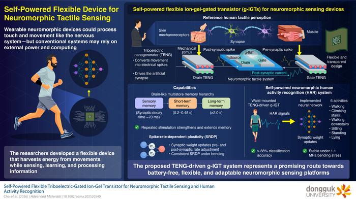
The proposed TENG-driven g-IGT is a flexible, self-powered neuromorphic device capable of reproducing multiple memory states and spike-rate-dependent learning Neuromorphic devices, which are designed to emulate aspects of biological neural networks, are promising candidates for developing low-power and intelligent sensing technologies, including wearable applications. Among the device architectures explored for neuromorphic computing, graphene-channel ion-gel-gated transistors (g-IGTs) are...
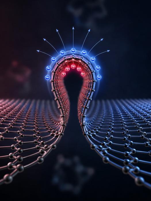
Rice University researchers have shown that sub-nanometer wrinkles in graphene generate flexoelectric charge separation, reshaping local electrical behavior through curvature alone. Extreme bending produces polarization far stronger than in larger systems and may enable geometry-controlled electronics without chemical doping. Published in Advanced Materials.
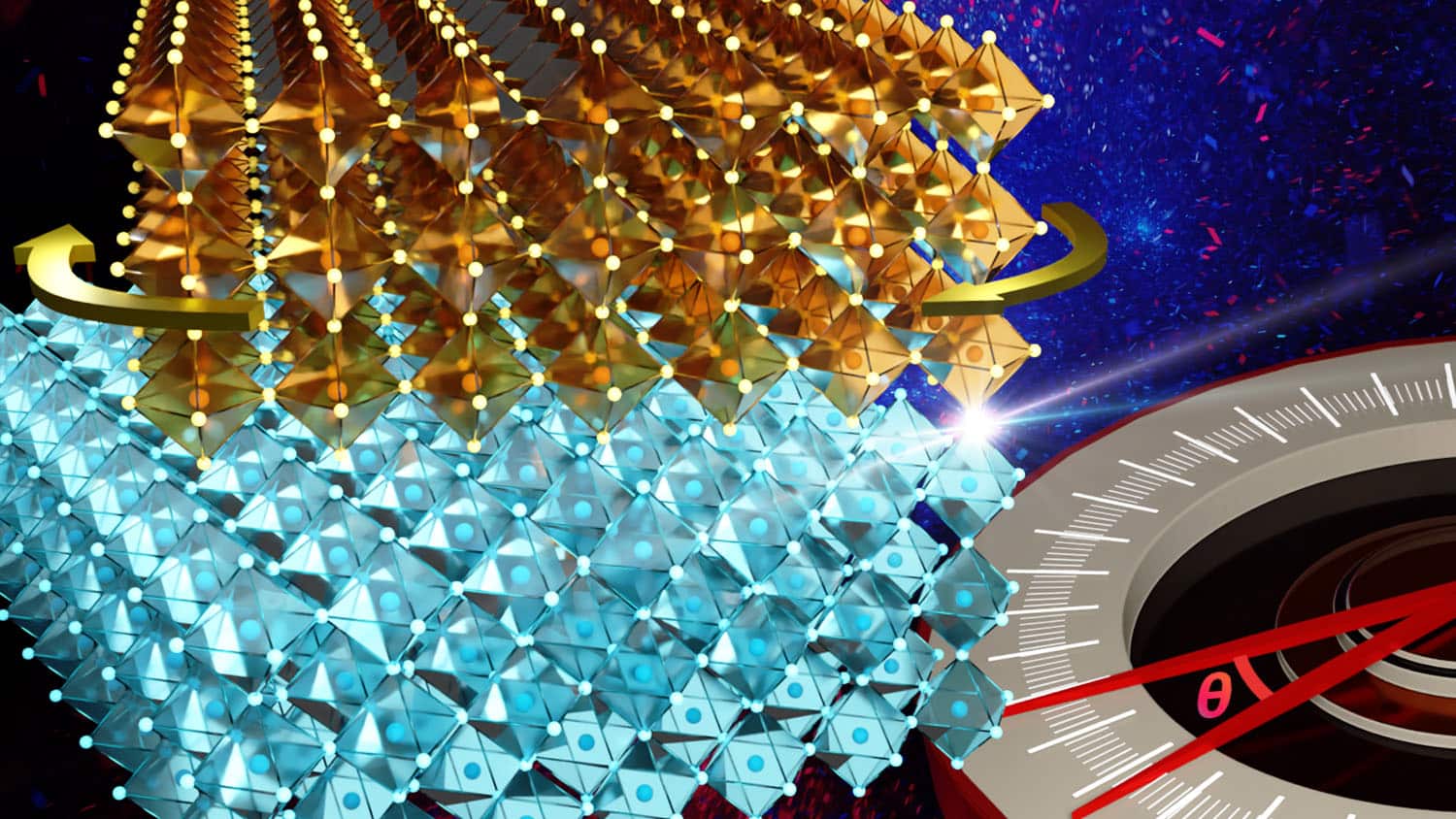
Researchers at NC State have extended twistronics beyond van der Waals materials into strongly bonded crystalline oxides. By stacking sodium niobate membranes with twist angles controlled down to 0.1 degrees, and confirming results via synchrotron X-ray diffraction, the team found interlayer bonds distort the atomic lattice, shifting phase structure and domain configuration. The technique works at near-millimeter scale, far larger than typical twistronic devices, marking a real step toward pract
