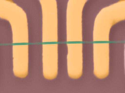
Engineers at the University of California, Riverside, have demonstrated prototype devices made of an exotic material that can conduct a current density 50 times greater than conventional copper interconnect technology.
Current density is the amount of electrical current per cross-sectional area at a given point. As transistors in integrated circuits become smaller and smaller, they need higher and higher current densities to perform at the desired level. Most conventional electrical conductors, such as copper, tend to break due to overheating or other factors at high current densities, presenting a barrier to creating increasingly small components.
The electronics industry needs alternatives to silicon and copper that can sustain extremely high current densities at sizes of just a few nanometers.
The advent of graphene resulted in a massive, worldwide effort directed at investigation of other two-dimensional, or 2D, layered materials that would meet the need for nanoscale electronic components that can sustain a high current density. While 2D materials consist of a single layer of atoms, 1D materials consist of individual chains of atoms weakly bound to one another, but their potential for electronics has not been as widely studied.
One can think of 2D materials as thin slices of bread while 1D materials are like spaghetti. Compared to 1D materials, 2D materials seem huge.
A group of researchers led by Alexander A. Balandin, a distinguished professor of electrical and computer engineering in the Marlan and Rosemary Bourns College of Engineering at UC Riverside, discovered that zirconium tritelluride, or ZrTe3, nanoribbons have an exceptionally high current density that far exceeds that of any conventional metals like copper.
The new strategy undertaken by the UC Riverside team pushes research from two-dimensional to one-dimensional materials-- an important advance for the future generation of electronics.
"Conventional metals are polycrystalline. They have grain boundaries and surface roughness, which scatter electrons," Balandin said. "Quasi-one-dimensional materials such as ZrTe3consist of single-crystal atomic chains in one direction. They do not have grain boundaries and often have atomically smooth surfaces after exfoliation. We attributed the exceptionally high current density in ZrTe3 to the single-crystal nature of quasi-1D materials."
In principle, such quasi-1D materials could be grown directly into nanowires with a cross-section that corresponds to an individual atomic thread, or chain. In the present study the level of the current sustained by the ZrTe3 quantum wires was higher than reported for any metals or other 1D materials. It almost reaches the current density in carbon nanotubes and graphene.
Electronic devices depend on special wiring to carry information between different parts of a circuit or system. As developers miniaturize devices, their internal parts also must become smaller, and the interconnects that carry information between parts must become smallest of all. Depending on how they are configured, the ZrTe3 nanoribbons could be made into either nanometer-scale local interconnects or device channels for components of the tiniest devices.
The UC Riverside group's experiments were conducted with nanoribbons that had been sliced from a pre-made sheet of material. Industrial applications need to grow nanoribbon directly on the wafer. This manufacturing process is already under development, and Balandin believes 1D nanomaterials hold possibilities for applications in future electronics.
"The most exciting thing about the quasi-1D materials is that they can be truly synthesized into the channels or interconnects with the ultimately small cross-section of one atomic thread-- approximately one nanometer by one nanometer," Balandin said.
Current Carrying Capacity of Quasi-1D ZrTe3 Van Der Waals Nanoribbons
A. Geremew; M. A. Bloodgood; E. Aytan; B. W. K. Woo; S. R. Corber; G. Liu; K. Bozhilov; T. T. Salguero; S. Rumyantsev; M. P. Rao; A. A. Balandin
IEEE Electron Device Letters (Volume: 39, Issue: 5)
DOI: 10.1109/LED.2018.2820140
University of California, Riverside
#Nanoelectronics #Nanomaterials #Nanoengineering #Semiconductors
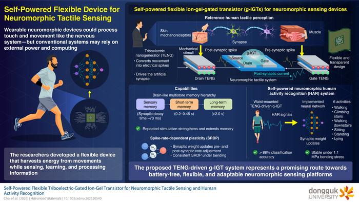
The proposed TENG-driven g-IGT is a flexible, self-powered neuromorphic device capable of reproducing multiple memory states and spike-rate-dependent learning Neuromorphic devices, which are designed to emulate aspects of biological neural networks, are promising candidates for developing low-power and intelligent sensing technologies, including wearable applications. Among the device architectures explored for neuromorphic computing, graphene-channel ion-gel-gated transistors (g-IGTs) are...
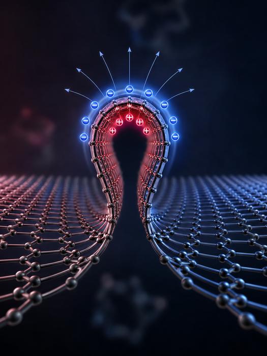
Rice University researchers have shown that sub-nanometer wrinkles in graphene generate flexoelectric charge separation, reshaping local electrical behavior through curvature alone. Extreme bending produces polarization far stronger than in larger systems and may enable geometry-controlled electronics without chemical doping. Published in Advanced Materials.
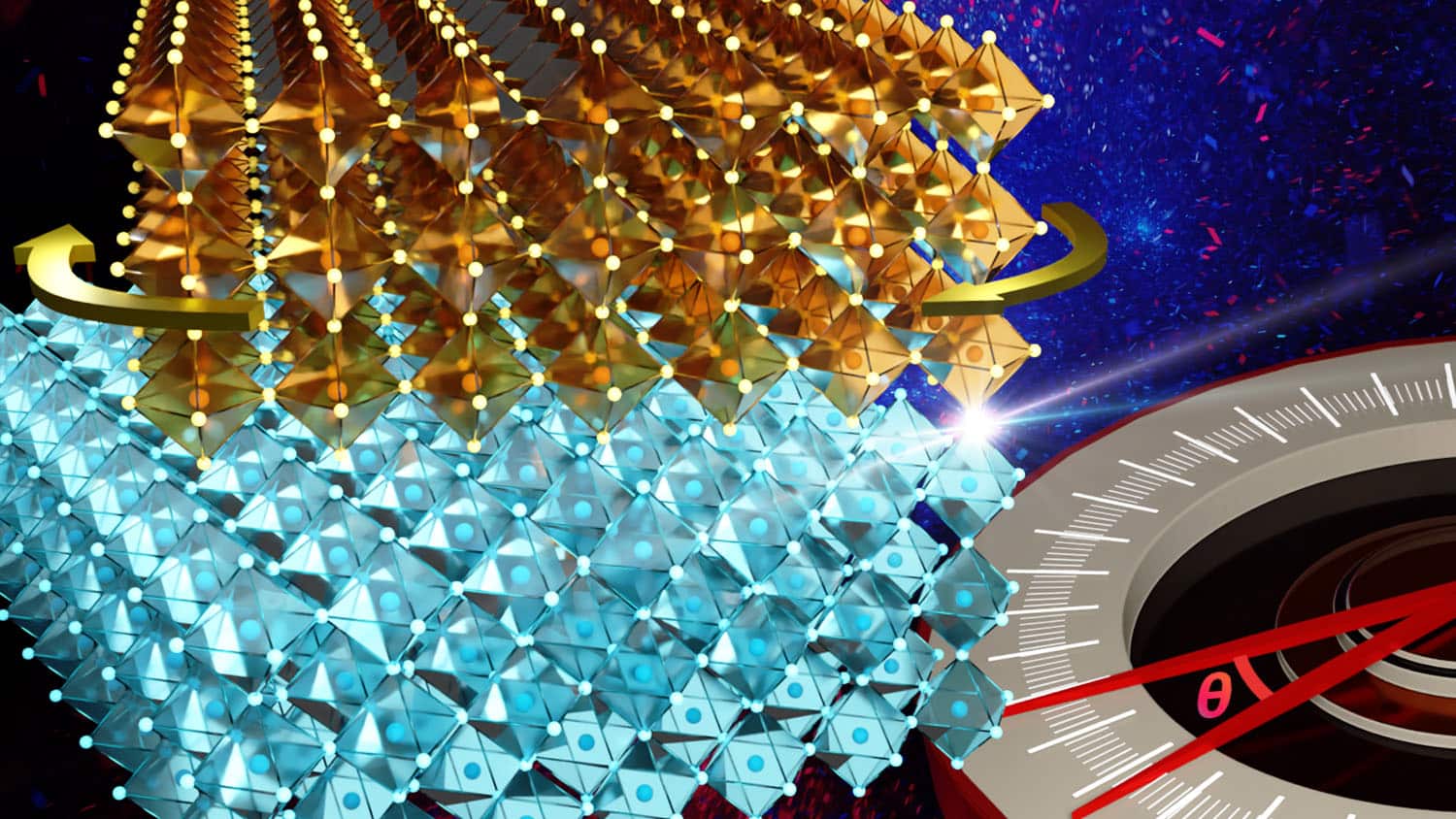
Researchers at NC State have extended twistronics beyond van der Waals materials into strongly bonded crystalline oxides. By stacking sodium niobate membranes with twist angles controlled down to 0.1 degrees, and confirming results via synchrotron X-ray diffraction, the team found interlayer bonds distort the atomic lattice, shifting phase structure and domain configuration. The technique works at near-millimeter scale, far larger than typical twistronic devices, marking a real step toward pract
