The Science
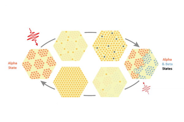
To better store data, scientists need ways to change a material’s properties suddenly. For example, they want a material that can go from insulator to conductor and back again. Now, they devised a surprisingly simple way of flipping a material from one state into another, and back again, with flashes of light. A single light pulse turns thin sheets of tantalum disulfide from its original (alpha) state into a mixture of alpha and beta states. Domain walls separate the two states. A second pulse of light dissolves the walls, and the material returns to its original state.
The Impact
The material’s new properties result from emerging patterns of electrons. Scientists can use these changes in electron charge distributions to build novel computers and more. Today’s computers manipulate the magnetic spin for data storage. This work shows that scientists could use the electron charge density to create pathways for new electronic devices.
Summary
Switching the configurations of electrons in a way that changes a material’s properties is key to information storage, processing, and transmission. Scientists have demonstrated new ultra-fast laser pulse techniques to change the charge ripples that exist in a material. The ripples, known as charge density waves, result from the quantum interactions of electrons and lattice vibrations. The long-range electron patterning creates “super-lattice” signatures, which can be measured with electron and X-ray scattering.
Scientists studied ultra-thin tantalum disulfide, which consists of layers of tantalum atoms sandwiched by sulfur atoms. Some of the electron charge normally associated with the locations of the atoms bunches up like peaks and troughs of waves, in positions and angles that are not completely aligned with the atomic structure. These electron density waves have two possible orientations, which the researchers switched using short bursts of laser light. When the light is strong enough, photo-induced defects in the system induce one orientation or the other at different locations. Eventually the oriented regions meet at boundary walls. These walls are expected to have different properties than the bulk material and might, for example, be used to switch the material from an insulator to a conductor at low temperature. To remove these walls, the scientists used a less intense pulse of light to return the material to a single orientation. The researchers plan to investigate the use of photoexcitation to perform ultrafast domain wall engineering and thus control materials properties in a switchable way on extremely short time scales, possibly leading to new quantum level electronic devices.
Ultrafast manipulation of mirror domain walls in a charge density wave
Alfred Zong, Xiaozhe Shen, Anshul Kogar, Linda Ye, Carolyn Marks, Debanjan Chowdhury, Timm Rohwer, Byron Freelon, Stephen Weathersby, Renkai Li, Jie Yang, Joseph Checkelsky, Xijie Wang and Nuh Gedik
Science Advances Vol. 4, no. 10
Massachusetts Institute of Technology (MIT) via DOE NEWS
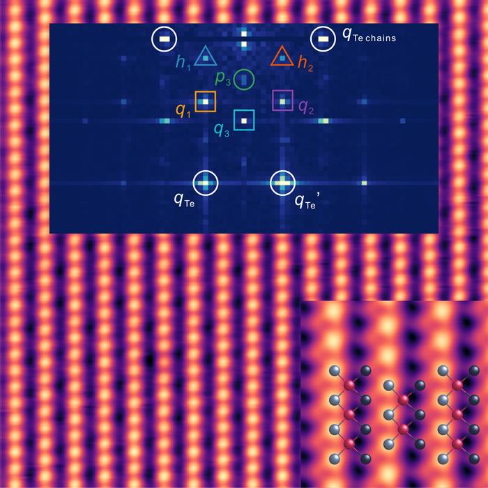
A Fourier transform revealing spatial patterns on the surface at 300 millikelvins. A charge density wave signals the presence of the pair density wave. The background is tellurium atoms on the surface of uranium ditelluride. @University of Illinois Urbana-Champaign’s Grainger College of Engineering Physicists with the University of Illinois Urbana-Champaign’s Grainger College of Engineering have identified a new form of superconducting behavior. Experiments on the metal uranium ditelluride...
Stack two atomically thin layers, rotate one slightly against the other, and a new material emerges. The resulting moiré pattern can slow electrons down so much that their interactions take over. This produces superconductivity, magnetism and exotic fractional quantum states that neither layer shows on its own. This field, known as twistronics, has become one of the most active frontiers in condensed matter physics. So far, however, it has been built on only a handful of materials, mainly...
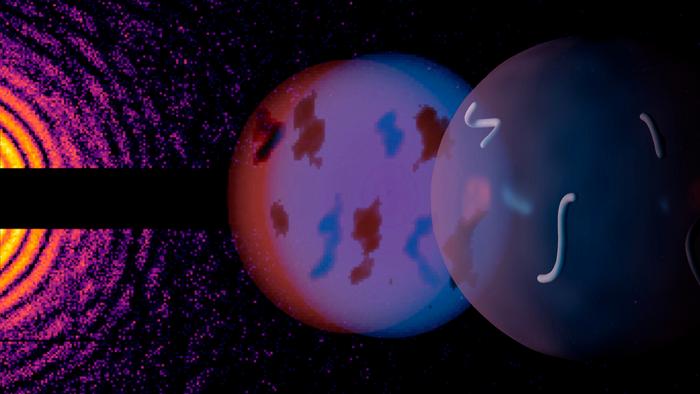
From a two-colour diffraction pattern (left), two snapshots of a helium droplet doped with xenon nanoparticles can be reconstructed (centre). These images can inform a potential 3D rendering of a xenon-doped helium nanodroplet (right). An overarching goal of ultrafast science is to enable researchers to watch structural changes in matter on their natural timescale. Experimentally, this translates into taking two snapshots of the same nanoscale object that are only femtoseconds apart to...
