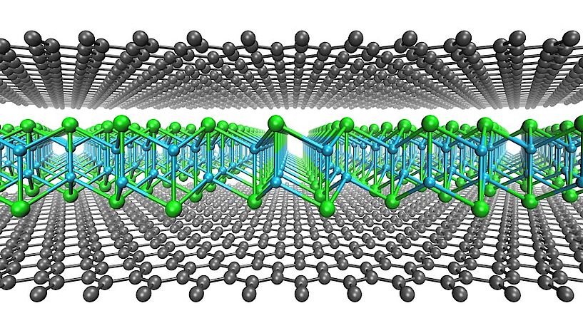
Atoms bind together by sharing electrons. The way this happens depends on the atom types but also on conditions such as temperature and pressure. In two-dimensional (2D) materials, such as graphene, atoms join along a plane to form structures just one atom thick, which leads to fascinating properties determined by quantum mechanics. Researchers at the University of Vienna in collaboration with the Universities of Tübingen, Antwerp and CY Cergy Paris, together with Danubia NanoTech, have produced a new 2D material made of copper and iodine atoms sandwiched between two graphene sheets. The results were published in the journal Advanced Materials.
The design of new materials allows for either improved efficiency of known applications or totally new applications that were out of reach with the previously existing materials. Indeed, tens of thousands of conventional materials such as metals and their alloys have been identified over the last hundred years. A similar number of possible 2D materials have been predicted to exist, but as of now, only a fraction of them have been produced in experiments. One reason for this is the instability of many of these materials in laboratory conditions.
In the recent study, the researchers synthesized 2D cuprous iodide that was stabilized in a graphene sandwich, as the first example of a material that does not otherwise exist in normal laboratory conditions. The synthesis utilizes the large interlayer spacing of oxidized graphene multilayers, which allows iodine and copper atoms to diffuse into the gap and to grow the new material. The graphene layers here have an important role imposing a high pressure on the sandwiched material that thus becomes stabilized. The resulting sandwich structure is shown in the illustration.
"As so often, when we first saw the new material in our microscopy images, it was a surprise", says Kimmo Mustonen, the lead author of the study. "It took us quite some time to figure out what the structure precisely was. This enabled us together with Danubia NanoTech company, headed by Viera Skákalová, to design a chemical process for producing it in large scale", he continues. Understanding the structure was a joint effort of scientists from the Universities of Vienna, Tübingen, Antwerp and CY Cergy Paris. "We had to use several electron microscopy techniques to make sure that we were really seeing a monolayer of copper and iodine and to extract the exact atom positions in 3D, including the latest methods we have recently developed", the second lead author Christoph Hofer adds.
Following the 2D copper iodide, the researchers have already expanded the synthesis method to produce other new 2D materials. "The method seems to be truly universal, providing access to dozens of new 2D materials. These are truly exciting times!", Kimmo Mustonen concludes.
Reference
Toward Exotic Layered Materials: 2D Cuprous Iodide
Kimmo Mustonen, Christoph Hofer, Peter Kotrusz, Alexander Markevich, Martin Hulman, Clemens Mangler, Toma Susi, Timothy J. Pennycook, Karol Hricovini, Christine Richter, Jannik C. Meyer, Jani Kotakoski, Viera Skákalová
https://onlinelibrary.wiley.com/doi/full/10.1002/adma.202106922
University of Vienna

Waste polyamide-derived CQDs show continuous photoluminescence tuning from 308 to 552 nm through sequential defect-state engineering, with optical transition energies decreasing from 4.32 to 2.50 eV. @Christian Ebere Enyoh from Saitama University Carbon quantum dots (CQDs) are fluorescent carbon nanomaterials with potential applications in sensing, optoelectronics, displays, anti-counterfeiting, and environmental technologies. Their optical properties can be adjusted by modifying the carbon...

The researchers used circularly polarized light at normal incidence and found that helicity-dependent photocurrents appeared perpendicular to the crystal’s polarization but vanished when measured parallel to it, supporting a bulk origin of CPGE. @Institute of Science Tokyo The circular photogalvanic effect (CPGE), a phenomenon that generates helicity-dependent photocurrents in noncentrosymmetric materials, can originate purely from a crystal's internal structure without contribution from the...

Summary of gold nanoparticle growth programming in liposome based on localization of biomineralization peptide The position of biomineralization peptides within liposomes can influence how gold nanoparticles grow, reports a research team from Institute of Science Tokyo. Peptides localized at the membrane interface promote branched structures, while those confined to the liposome interior favor spherical nanoparticles. The findings offer a new strategy for controlling nanoscale reaction...
