Helmholtz-Zentrum Berlin für Materialien und Energie (HZB)
Microelectronics utilise various functional materials whose properties make them suitable for specific applications. For example, transistors and data storage devices are made of silicon, and most photovoltaic cells used for generating electricity from sunlight are also currently made of this semiconductor material. In contrast, compound semiconductors such as gallium nitride are used to generate light in optoelectronic elements such as light-emitting diodes (LEDs). The manufacturing processes also different for the various classes of materials.
Transcending the materials and methods maze
Hybrid perovskite materials promise simplification - by arranging the organic and inorganic components of semiconducting crystal in a specific structure. "They can be used to manufacture all kinds of microelectronic components by modifying their composition", says Prof. Emil List-Kratochvil, head of a Joint Research Group at HZB and Humboldt-Universität.
What's more, processing perovskite crystals is comparatively simple. "They can be produced from a liquid solution, so you can build the desired component one layer at a time directly on the substrate", the physicist explains.
First solar cells from an inkjet printer, now light-emitting diodes too
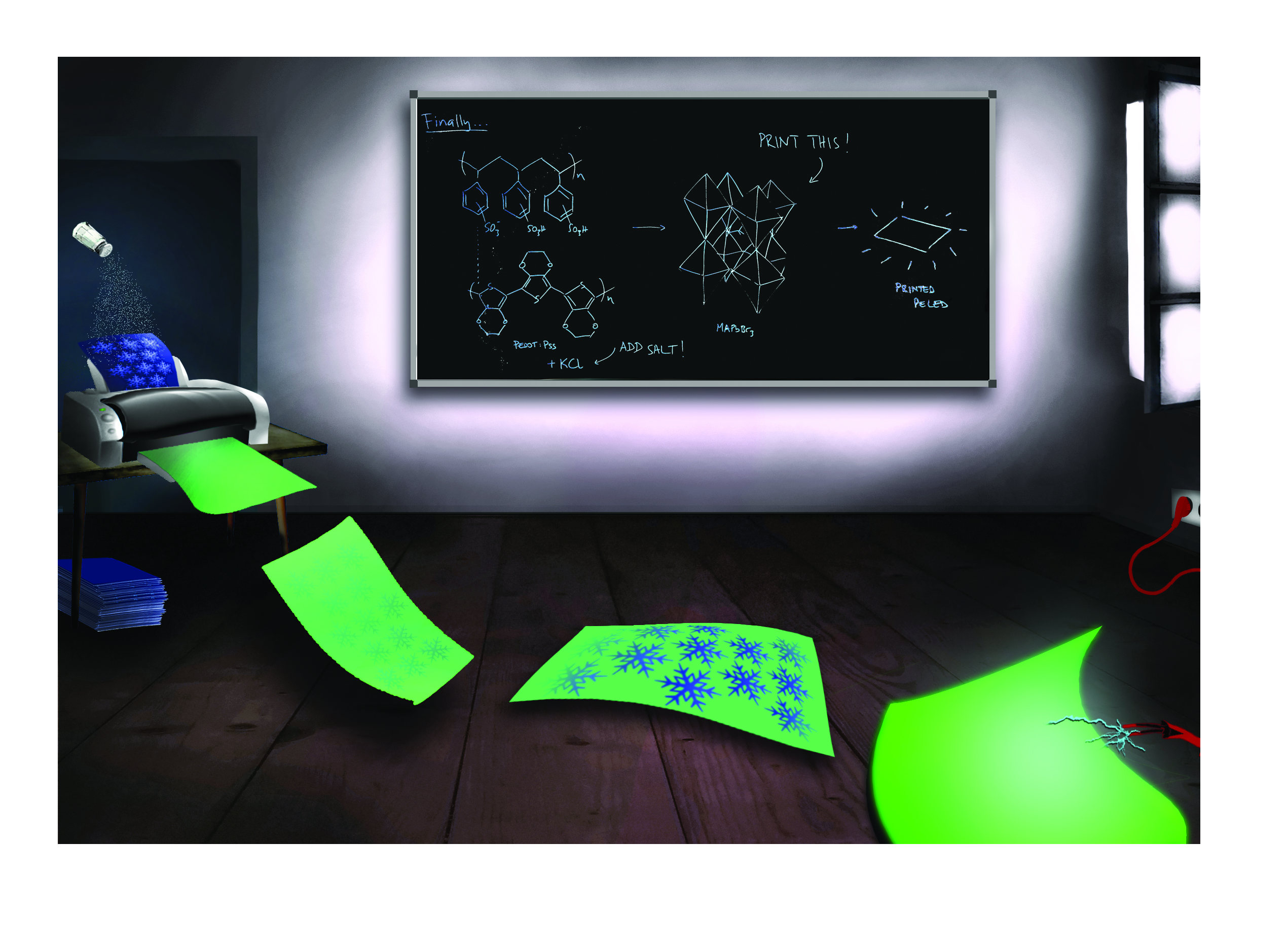
Scientists at HZB have already shown in recent years that solar cells can be printed from a solution of semiconductor compounds - and are worldwide leaders in this technology today. Now for the first time, the joint team of HZB and HU Berlin has succeeded in producing functional light-emitting diodes in this manner. The research group used a metal halide perovskite for this purpose. This is a material that promises particularly high efficiency in generating light - but on the other hand is difficult to process.
"Until now, it has not been possible to produce these kinds of semiconductor layers with sufficient quality from a liquid solution", says List-Kratochvil. For example, LEDs could be printed just from organic semiconductors, but these provide only modest luminosity. "The challenge was how to cause the salt-like precursor that we printed onto the substrate to crystallise quickly and evenly by using some sort of an attractant or catalyst", explains the scientist. The team chose a seed crystal for this purpose: a salt crystal that attaches itself to the substrate and triggers formation of a gridwork for the subsequent perovskite layers.
Significantly better optical and electronic characteristics
In this way, the researchers created printed LEDs that possess far higher luminosity and considerably better electrical properties than could be previously achieved using additive manufacturing processes. But for List-Kratochvil, this success is only an intermediate step on the road to future micro- and optoelectronics that he believes will be based exclusively on hybrid perovskite semiconductors. "The advantages offered by a single universally applicable class of materials and a single cost-effective and simple process for manufacturing any kind of component are striking", says the scientist. He is therefore planning to eventually manufacture all important electronic components this way in the laboratories of HZB and HU Berlin.
List-Kratochvil is Professor of Hybrid Devices at the Humboldt-Universität zu Berlin and head of a Joint Lab founded in 2018 that is operated by HU together with HZB. In addition, a team jointly headed by List-Kratochvil and HZB scientist Dr. Eva Unger is working in the Helmholtz Innovation Lab HySPRINT on the development of coating and printing processes - also known in technical jargon as "additive manufacturing" - for hybrid perovskites. These are crystals possessing a perovskite structure that contain both inorganic and organic components.
Finally, inkjet-printed metal halide perovskite LEDs – utilizing seed crystal templating of salty PEDOT:PSS
Felix Hermerschmidt, Florian Mathies, Vincent R. F. Schröder, Carolin Rehermann, Nicolas Zorn Morales, Eva L. Unger and Emil J. W. List-Kratochvi
Materials Horizons (2020)
DOI: 10.1039/D0MH00512F
Contact information:
Eva Unger
eva.unger@helmholtz-berlin.de
Phone: +49 (030) 8062 - 13116
Florian Mathies
florian.mathies@helmholtz-berlin.de
Phone: +49 (030) 8062 - 13118
Emil List-Kratochvil
emil.list-kratochvil@hu-berlin.de
Phone: +49 (030) 2093 7697
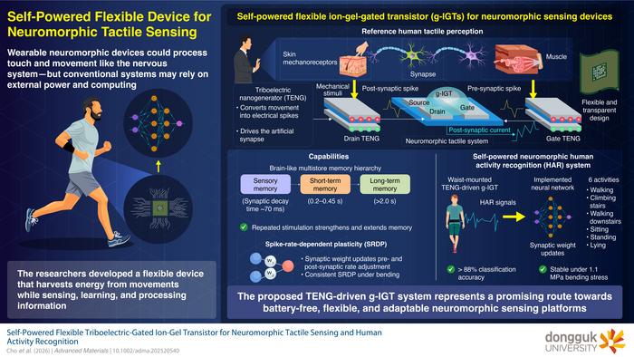
The proposed TENG-driven g-IGT is a flexible, self-powered neuromorphic device capable of reproducing multiple memory states and spike-rate-dependent learning Neuromorphic devices, which are designed to emulate aspects of biological neural networks, are promising candidates for developing low-power and intelligent sensing technologies, including wearable applications. Among the device architectures explored for neuromorphic computing, graphene-channel ion-gel-gated transistors (g-IGTs) are...
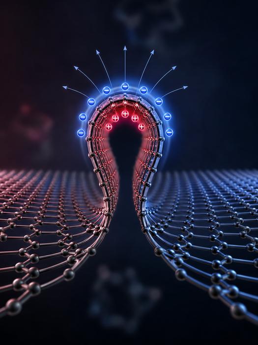
Rice University researchers have shown that sub-nanometer wrinkles in graphene generate flexoelectric charge separation, reshaping local electrical behavior through curvature alone. Extreme bending produces polarization far stronger than in larger systems and may enable geometry-controlled electronics without chemical doping. Published in Advanced Materials.
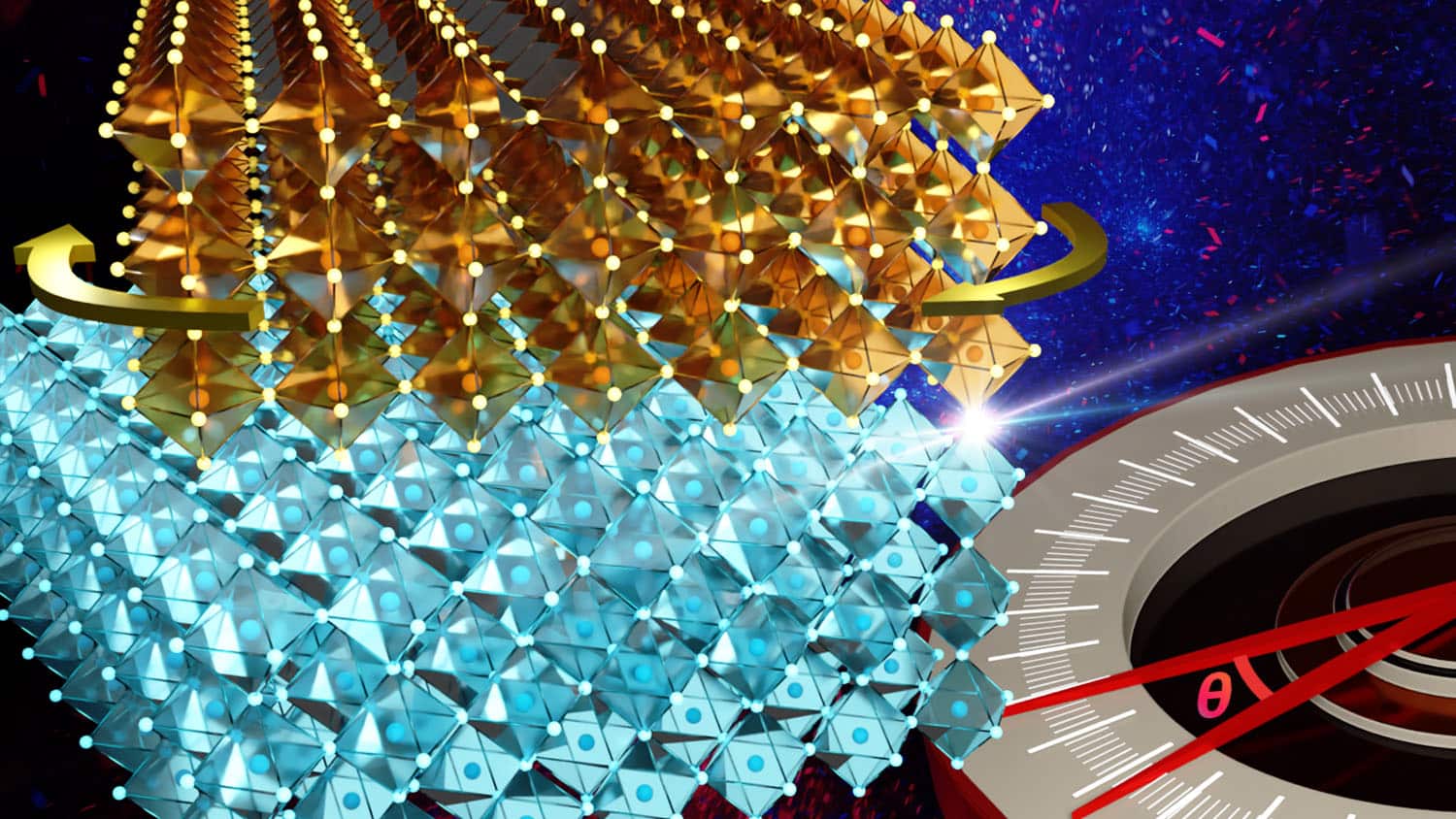
Researchers at NC State have extended twistronics beyond van der Waals materials into strongly bonded crystalline oxides. By stacking sodium niobate membranes with twist angles controlled down to 0.1 degrees, and confirming results via synchrotron X-ray diffraction, the team found interlayer bonds distort the atomic lattice, shifting phase structure and domain configuration. The technique works at near-millimeter scale, far larger than typical twistronic devices, marking a real step toward pract
