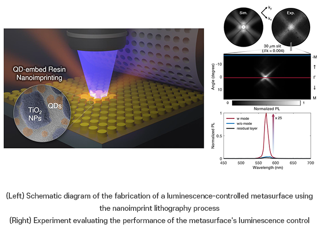
In relationships, sharing closer spaces naturally deepens the connection as bonds form and strengthen through increasing shared memories. This principle applies not only to human interactions but also to engineering. Recently, an intriguing study was published demonstrating the use of quantum dots to create metasurfaces, enabling two objects to exist in the same space.
Professor Junsuk Rho from the Department of Mechanical Engineering, the Department of Chemical Engineering, and the Department of Electrical Engineering, PhD candidates Minsu Jeong, Byoungsu Ko, and Jaekyung Kim from the Department of Mechanical Engineering, and Chunghwan Jung, a PhD candidate, from the Department of Chemical Engineering at Pohang University of Science and Technology (POSTECH) employed Nanoimprint Lithography (NIL) to fabricate metasurfaces embedded with quantum dots, enhancing their luminescence efficiency. Their research was recently published in the online edition of “Nano Letters”, an international journal in nanotechnology.
NIL, a process for creating optical metasurfaces, utilizes patterned stamps to quickly transfer intricate patterns at the nanometer (nm) scale. This method offers cost advantages over electron beam lithography and other processes and has the advantage of enabling the creation of metasurfaces using materials that are not available in conventional processes.
Metasurfaces have recently been the focus of extensive research for their ability to control the polarization and emission direction of light from quantum dots. Quantum dots, which are nanoscale semiconductor particles, are highly efficient light emitters capable of emitting light at precise wavelengths. This makes them widely used in applications such as QLEDs and quantum computing. However, conventional processes cannot embed quantum dots within metasurfaces. As a result, research has often involved fabricating metasurfaces and quantum dots separately and then combining them, which imposes limitations on controlling the luminescence of the quantum dots.
In this study, the researchers integrated quantum dots with titanium dioxide (TiO2), a material used in the NIL process, to create a metasurface. Unlike conventional methods, which involve separately fabricating the metasurface and quantum dots before combining them, this approach embeds the quantum dots directly within the metasurface during its creation.
The resulting metasurface enhances the proportion of photons emitted from the quantum dots that couple with the resonance mode of the metasurface. This advancement allows for more effective control over the specific direction of light emitted from the quantum dots compared to previous methods.
Experiments demonstrated that the more photons emitted from the quantum dots that were coupled to the resonant modes of the metasurface, the higher the luminescence efficiency. The team’s metasurface achieved up to 25 times greater luminescence efficiency compared to a simple coating of quantum dots.
Professor Junsuk Rho of POSTECH who led the research stated, “The use of luminescence-controlled metasurfaces will enable sharper, brighter displays and more precise, sensitive biosensing.” He added, “Further research will allow us to control luminescence more effectively, leading to advances in areas such as nano-optical sensors, optoelectronic devices, and quantum dot displays.”
Reference
Printable Light-Emitting Metasurfaces with Enhanced Directional Photoluminescence
Minsu Jeong, Byoungsu Ko, Chunghwan Jung, Jaekyung Kim, Jaehyuck Jang, Jungho Mun, Jihae Lee, Suhyeon Yun, Sejeong Kim, and Junsuk Rho
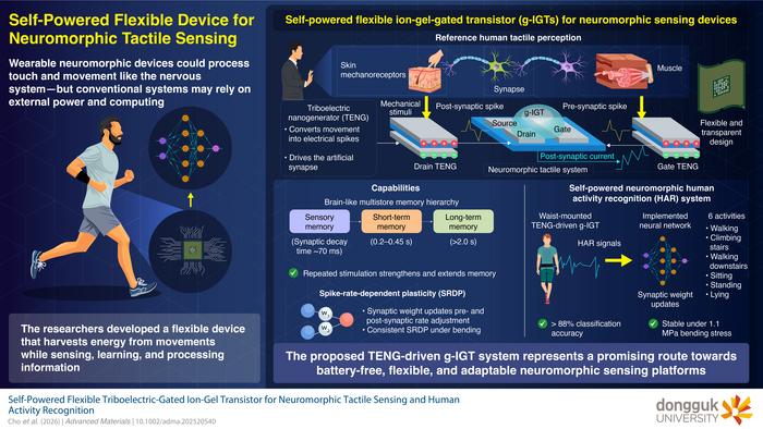
The proposed TENG-driven g-IGT is a flexible, self-powered neuromorphic device capable of reproducing multiple memory states and spike-rate-dependent learning Neuromorphic devices, which are designed to emulate aspects of biological neural networks, are promising candidates for developing low-power and intelligent sensing technologies, including wearable applications. Among the device architectures explored for neuromorphic computing, graphene-channel ion-gel-gated transistors (g-IGTs) are...
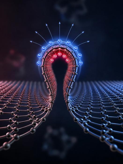
Rice University researchers have shown that sub-nanometer wrinkles in graphene generate flexoelectric charge separation, reshaping local electrical behavior through curvature alone. Extreme bending produces polarization far stronger than in larger systems and may enable geometry-controlled electronics without chemical doping. Published in Advanced Materials.
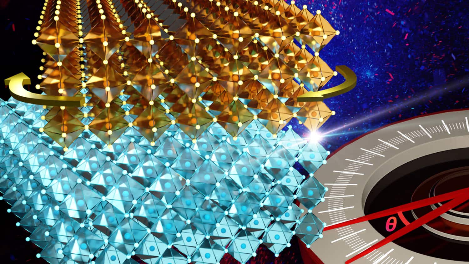
Researchers at NC State have extended twistronics beyond van der Waals materials into strongly bonded crystalline oxides. By stacking sodium niobate membranes with twist angles controlled down to 0.1 degrees, and confirming results via synchrotron X-ray diffraction, the team found interlayer bonds distort the atomic lattice, shifting phase structure and domain configuration. The technique works at near-millimeter scale, far larger than typical twistronic devices, marking a real step toward pract
