Two-dimensional (2D) materials, which consist of a single layer of atoms, have attracted a lot of attention since the isolation of graphene in 2004. They have unique electrical, optical, and mechanical properties, like high conductivity, flexibility and strength, which makes them promising materials for such things as lasers, photovoltaics, sensors and medical applications.
When a sheet of 2D material is placed over another and slightly rotated, the twist can radically change the bilayer material's properties and lead to exotic physical behaviours, such as high temperature superconductivity - exiting for electrical engineering; nonlinear optics - exciting for lasers and data transmission; and structural super-lubricity- a newly discovered mechanical property which researchers are only beginning to understand. The study of these properties has given birth to a new field of research called twistronics, so-called because it's a combination of twist and electronics.
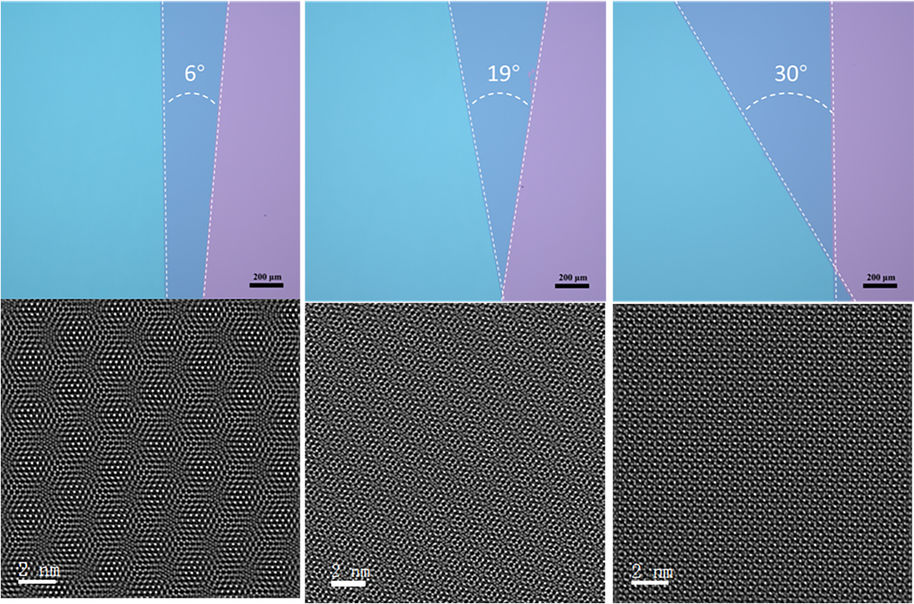
Aalto University's researchers collaborating with international colleagues have now developed a new method for making these twisted layers on scales that are large enough to be useful, for the first time. Their new method for transferring single-atom layers of molybdenum disulfide (MoS2) allows researchers to precisely control the twist angle between layers with up to a square centimetre in area, making it record-breaking in terms of size. Controlling the interlayer twist angle on a large scale is crucial for the future practical applications of twistronics.
'Our demonstrated twist method allows us to tune the properties of stacked multilayer MoS2 structures on larger scales than ever before. The transfer method can also apply to other two-dimensional layered materials', says Dr Luojun Du from Aalto University, one of the lead authors of the work.
A significant advancement for a brand-new field of research
Since twistronics research was introduced only in 2018, basic research is still needed to understand the properties of twisted materials better before they find their ways to practical applications. The Wolf Prize in Physics, one of the most prestigious scientific awards, was awarded to Profs. Rafi Bistritzer, Pablo Jarillo-Herrero, and Allan H. MacDonald this year for their groundbreaking work on twistronics, which indicates the game-changing potential of the emerging field.
Previous research has demonstrated that it is possible to fabricate the required twist angle by transfer method or atomic force microscope tip manipulation techniques in small scales. The sample size has usually been in the order of ten-microns, less than the size of a human hair. Larger few-layer films have also been fabricated, but their interlayer twist angle is random. Now the researchers can grow large films using an epitaxial growth method and water assistant transfer method.
'Since no polymer is needed during the transfer process, the interfaces of our sample are relatively clean. With the control of twist angle and ultra-clean interfaces, we could tune the physical properties, including low-frequency interlayer modes, band structure, and optical and electrical properties', Du says.
'Indeed, the work is of great significance in guiding the future applications of twistronics based on 2D materials', adds Professor Zhipei Sun from Aalto University.
Precise control of the interlayer twist angle in large scale MoS2 homostructures
Mengzhou Liao, Zheng Wei, Luojun Du, Qinqin Wang, Jian Tang, Hua Yu, Fanfan Wu, Jiaojiao Zhao, Xiaozhi Xu, Bo Han, Kaihui Liu, Peng Gao, Tomas Polcar, Zhipei Sun, Dongxia Shi, Rong Yang & Guangyu Zhang
Nature Communications volume 11, Article number: 2153 (2020)
DOI: 10.1038/s41467-020-16056-4
Contact information:
Luojun Du
Aalto Postdoctoral researcher, Department of Electronics & Nanoengineering
luojun.du@aalto.fi
Zhipei Sun
Aalto Professor, Department of Electronics & Nanoengineering
zhipei.sun@aalto.fi
Phone: +358 50 430 2820
Aalto University

Waste polyamide-derived CQDs show continuous photoluminescence tuning from 308 to 552 nm through sequential defect-state engineering, with optical transition energies decreasing from 4.32 to 2.50 eV. @Christian Ebere Enyoh from Saitama University Carbon quantum dots (CQDs) are fluorescent carbon nanomaterials with potential applications in sensing, optoelectronics, displays, anti-counterfeiting, and environmental technologies. Their optical properties can be adjusted by modifying the carbon...

The researchers used circularly polarized light at normal incidence and found that helicity-dependent photocurrents appeared perpendicular to the crystal’s polarization but vanished when measured parallel to it, supporting a bulk origin of CPGE. @Institute of Science Tokyo The circular photogalvanic effect (CPGE), a phenomenon that generates helicity-dependent photocurrents in noncentrosymmetric materials, can originate purely from a crystal's internal structure without contribution from the...

Summary of gold nanoparticle growth programming in liposome based on localization of biomineralization peptide The position of biomineralization peptides within liposomes can influence how gold nanoparticles grow, reports a research team from Institute of Science Tokyo. Peptides localized at the membrane interface promote branched structures, while those confined to the liposome interior favor spherical nanoparticles. The findings offer a new strategy for controlling nanoscale reaction...
