Korea Institute of Science and Technology
We live in an era of data deluge. The data centers that are operated to store and process this flood of data use a lot of electricity, which has been called a major contributor to environmental pollution. To overcome this situation, polygonal computing systems with lower power consumption and higher computation speed are being researched, but they are not able to handle the huge demand for data processing because they operate with electrical signals, just like conventional binary computing systems.
The Korea Institute of Science and Technology (KIST, President Seok Jin Yoon) announced that Dr. Do Kyung Hwang of the Center for Opto-Electronic Materials & Devices and Professor Jong-Soo Lee of the Department of Energy Science & Engineering at Daegu Gyeongbuk Institute of Science and Technology (DGIST, President Young Kuk) has jointly developed a new zero-dimensional and two-dimensional (2D-0D) semiconductor artificial junction material and observed the effect of a next-generation memory powered by light. Transmitting data between the computing and storage parts of a multi-level computer using light rather than electrical signals can dramatically increase processing speed.
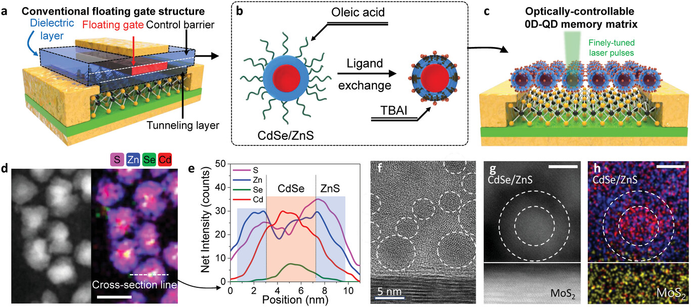
The research team has fabricated a new 2D-0D semiconductor artificial junction material by joining quantum dots in a core-shell structure with zinc sulfide (ZnS) on the surface of cadmium selenide (CdSe) and a molybdenum sulfide (MoS2) semiconductor. The new material enables the storage and manipulation of electronic states within quantum dots measuring 10 nm or less.
When light is applied to the cadmium selenide core, a certain number of electrons flow out of the molybdenum sulfide semiconductor, trapping holes in the core and making it conductive. The electron state inside cadmium selenide is also quantized. Intermittent light pulses trap electrons in the electron band one after the other, inducing a change in the resistance of the molybdenum sulfide through the field effect, and the resistance changes in a cascading manner depending on the number of light pulses. This process makes it possible to divide and maintain more than 0 and 10 states, unlike conventional memory, which has only 0 and 1 states. The zinc sulfide shell also prevents charge leakage between neighboring quantum dots, allowing each single quantum dot to function as a memory.
While quantum dots in conventional 2D-0D semiconductor artificial junction structures simply amplify signals from light sensors, the team's quantum dot structure perfectly mimics the floating gate memory structure, confirming its potential for use as a next-generation optical memory. The researchers verified the effectiveness of the polynomial memory phenomenon with neural network modeling using the CIFAR-10 dataset and achieved a 91% recognition rate.
Dr. Hwang of KIST said, "The new multi-level optical memory device will contribute to accelerating the industrialization of next-generation system technologies such as artificial intelligence systems, which have been difficult to commercialize due to technical limitations arising from the miniaturization and integration of existing silicon semiconductor devices."
Reference
Probing Optical Multi-Level Memory Effects in Single Core-Shell Quantum Dots and Application Through 2D–0D Hybrid Inverters
Hyun-Soo Ra, Tae Wook Kim, Derrick Allan Taylor, Je-Jun Lee, Seungho Song, Jongtae Ahn, Jisu Jang, Takashi Taniguchi, Kenji Watanabe, Jae Won Shim, Jong-Soo Lee, Do Kyung Hwang
The proposed TENG-driven g-IGT is a flexible, self-powered neuromorphic device capable of reproducing multiple memory states and spike-rate-dependent learning Neuromorphic devices, which are designed to emulate aspects of biological neural networks, are promising candidates for developing low-power and intelligent sensing technologies, including wearable applications. Among the device architectures explored for neuromorphic computing, graphene-channel ion-gel-gated transistors (g-IGTs) are...
Rice University researchers have shown that sub-nanometer wrinkles in graphene generate flexoelectric charge separation, reshaping local electrical behavior through curvature alone. Extreme bending produces polarization far stronger than in larger systems and may enable geometry-controlled electronics without chemical doping. Published in Advanced Materials.
Researchers at NC State have extended twistronics beyond van der Waals materials into strongly bonded crystalline oxides. By stacking sodium niobate membranes with twist angles controlled down to 0.1 degrees, and confirming results via synchrotron X-ray diffraction, the team found interlayer bonds distort the atomic lattice, shifting phase structure and domain configuration. The technique works at near-millimeter scale, far larger than typical twistronic devices, marking a real step toward pract
