Harvard John A. Paulson School of Engineering and Applied Sciences (SEAS)

Addressing a major roadblock in next-generation photonic computing and signal processing systems, researchers in the Harvard John A. Paulson School of Engineering and Applied Sciences (SEAS) have created a device that can bridge digital electronic signals and analog light signals in one fluid step.
Built on chips made out of lithium niobate, the workhorse material of optoelectronics, the new device offers a potential replacement for the ubiquitous but energy-intensive digital-to-analog conversion and electro-optic modulation systems used all over today’s high-speed data networks.
“Optical communication and high-performance computing, including large language models, rely on conversion of massive amounts of data between the electrical domain – used for storage and computation – and the optical domain – used for data transfer,” said senior author Marko Lončar, the Tiantsai Lin Professor of Electrical Engineering at SEAS.“For photonic technologies to seamlessly integrate with electronic ones, the interfaces between them must be fast and energy-efficient.”
The research is published in Nature Photonics.
Today’s photonic computing bottlenecks
Today, electronic digital-to-analog converters, followed by electro-optic modulators, accomplish the task of converting digital electronic signals into analog photonic signals, a process that underpins modern transceiver systems in data centers. But such a workflow is often complex, multi-tiered, and can be energy-intensive.
“When you’re computing with light, all the energy that you’ve saving, all the speed that you’re getting, tends to be offset by these big, expensive, inefficient electronic boxes that you need in order to take zeros and ones and turn them into a sine wave, square wave, triangle wave, or any meaningful waveform,” explained co-first author Yunxiang Song, graduate student in the Lončar Lab. “These things are actually the bottleneck in many types of photonic computing … So the question was, can we design some kind of novel photonic modulator that obviates the need for these electronic digital-to-analog converters?”
The new Harvard device offers just that. Making use of the efficient electro-optic properties of thin-film lithium niobate, it can turn purely digital electronic inputs into analog optical signals at information rates reaching up to 186 gigabits per second – an order of magnitude faster than typical home internet speeds. The device could also enable advances in microwave photonics, for example in wireless or radar communications, as it can be combined with photodetection to perform optical-to-electronic conversion for creating radio frequency signals.
Finally, emerging optical computing approaches, or computing using light rather than electrons, are of great interest because photons have the potential to process data in parallel and more efficiently than conventional electronics.
“Our work has the potential to address the current bottleneck of computing and data interconnects particularly in AI technologies,” said co-first author Yaowen Hu, former postdoctoral researcher at Harvard SEAS and now assistant professor at Peking University.
Demonstration of foundry process similar to silicon
To demonstrate that their device handles data with precision and speed, they tested it by optically encoding images from the well-known MNIST dataset, typically used to benchmark photonic computing systems.
The researchers’ device was fabricated using a lithium niobate foundry process, developed by Harvard startup HyperLight Corporation, that mirrors what exists for silicon chips, which are today in every phone and computer and upon which the digital revolution was built. The team thus showed not only that the device works for their particular application, but also that they can make it in a high-volume and low-cost manner, further paving the way for novel photonic technologies that can complement silicon photonics.
Reference
Integrated electro-optic digital-to-analogue link for efficient computing and arbitrary waveform generation
Yunxiang Song, Yaowen Hu, Xinrui Zhu, Keith Powell, Letícia Magalhães, Fan Ye, Hana K. Warner, Shengyuan Lu, Xudong Li, Dylan Renaud, Norman Lippok, Di Zhu, Benjamin Vakoc, Mian Zhang, Neil Sinclair & Marko Lončar
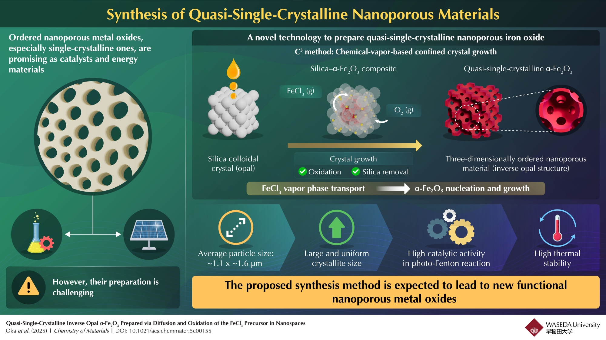
Nanoporous metal oxides have a wide variety of applications, such as catalysts, electrodes, energy materials, sensors, and biomaterials. Recently, a team of researchers has demonstrated a novel synthesis method for their efficient and desirable preparation. Specifically, they prepared difficult-to-prepare quasi-single-crystalline inverse opal α-Fe2O3, demonstrating that crystal growth occurs in nanospace due to volatilization and oxidation of metal chlorides. This technology is expected to fu...
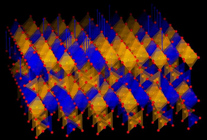
A team of scientists from Korea and Japan has discovered a new type of crystal that can "breathe"—releasing and absorbing oxygen repeatedly at relatively low temperatures. This unique ability could transform the way we develop clean energy technologies, including fuel cells, energy-saving windows, and smart thermal devices. The newly developed material is a special kind of metal oxide made of strontium, iron, and cobalt. What makes it extraordinary is that it can release oxygen when heated in...

Three nano glass spheres cling to one another. They form a tower-like cluster, similar to when you pile three scoops of ice cream on top of one another – only much smaller. The diameter of the nano cluster is ten times smaller than that of a human hair. With the help of an optical device and laser beams, researchers at ETH Zurich have succeeded in keeping such objects almost completely motionless in levitation. This is significant when it comes to the future development of quantum sensors, wh...
This week in nanotech
$10.2M raised
2 funding rounds · 19 deals tracked
New products
 Orion Sputtering Deposition SystemsAJA International Featured
 Nion-compatible In Situ STEM Holders for Electrical BiasingHummingbird Scientific Featured
 PDK (Process Design Kit)DB HiTek
Market insights
Last 30 days: Quantum Technologies was the busiest vertical: 55 of 182 events (30%).
Money raised per month