Stitching nanostrips together to create new 2D heterogeneous materials: a novel synthesis technique
- May 6, 2022
- 2 min read

New bidimensional (2D) materials with useful properties can be synthesised by stacking monoatomic layers of different chemical structure and composition, which bond via van der Waals forces. Interface phenomena emerge and the resulting heterostructures present characteristics that are different (and hopefully superior) to those of the constituent materials.
While vertical heterostructures are already commonly produced with relatively easy control over the process, the synthesis of lateral heterostructures –where different 2D atomic panels are ‘stitched’ one next to the other to form a single layer— presents additional challenges. In particular, the techniques used so far do not allow building heterostructures with atomic precision, and lattice mismatch and chemical instabilities at the interfaces compromise the outcome.
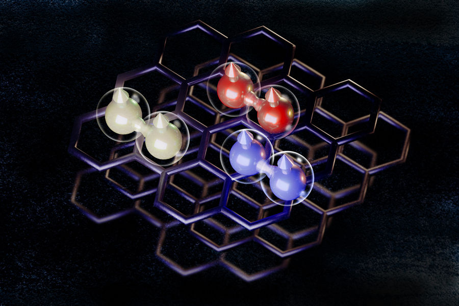
Researchers at the Catalan Institute of Nanoscience and Nanotechnology (ICN2, Spain), in collaboration with colleagues at the CiQUS centre of the University of Santiago de Campostela (Spain) and at the University of Cantabria (UNICAN, Spain), have developed a bottom-up synthesis method that enables the assembly of 2D lateral superlattice heterostructures, made of periodic arrays of heterojunctions between pristine and nitrogen-doped graphene nanoribbons. This study, published in Advanced Materials, was coordinated by ICREA Prof. Aitor Mugarza, leader of the ICN2 Atomic Manipulation and Spectroscopy Group, Dr César Moreno, former member of the same group and currently researcher at UNICAN, Dr Miguel Pruneda, from the ICN2 Theory and Simulation Group, and Dr Diego Peña, from CiQUS. First author of the paper is Dr Maria Tenorio, from Prof. Mugarza’s team.
By extending a technique developed at ICN2 by Prof. Mugarza’s group (and published in Science) to produce nanoporous graphene, the authors were able to synthesize single layers of hybrid nanoporous graphene with chemically heterogeneous pore structure, that electronically behave as a lateral superlattice heterostructure. The heterostructure exhibits a lattice period that can be as low as a nanometer –something never obtained before— and unprecedented discontinuities in the electronic bands down to the single-bond limit. Such properties endow this nanomaterial with a multifunctionality that can be exploited in photodetection, excitonic solar cells, water splitting, or selective nanofiltration.
The synthesis technique is a three-step procedure. Nanoribbons of the first component (pristine, undoped graphene) are grown over a surface (a gold layer with a specific lattice orientation), which acts as a template. The array of graphene nanoribbons obtained, in turn, dictates the arrangement of nanoribbons of the other component (N-doped graphene), which are synthesised in a second step. They grow in-between the undoped graphene strips, generating a pattern of intercalated components. After a third annealing step, a layer of hybrid nanoporous graphene with heterogeneous pore structure is obtained by their lateral fusion.
The new nanomaterial produced by means of this bottom-up technique behaves electronically as a 2D lateral superlattice heterostructure showing atomically precise interfaces and band discontinuities. The location of N atoms at specific sites of the pore edges is particularly relevant, since it can enhance selectivity in filtration or produce interactions at the pores that are crucial for sensing applications. Reference Atomically Sharp Lateral Superlattice Heterojunctions Built-In Nitrogen-Doped Nanoporous Graphene
Maria Tenorio, Cesar Moreno, Pol Febrer, Jesús Castro-Esteban, Pablo Ordejón, Diego Peña, Miguel Pruneda, Aitor Mugarza