Nanotechnology industry news & research highlights

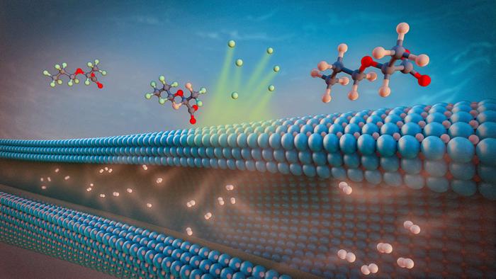
A UCLA-led team has extended a quantum phenomenon called the commensurate charge density wave in tantalum disulfide from cryogenic temperatures to roughly 135 F by interleaving layers of the amino acid arginine between ultrathin sheets. Two other amino acids failed to produce the effect, and simulations suggest arginine fits the crystal lattice almost perfectly. The work points to molecule-guided design of quantum materials and possible energy-efficient memory.
4 days ago · 4 min read
Oct 16 · 3 min read

Oct 9 · 4 min read
 Business
California Nanotechnologies has amended its Santa Ana lease to add 15,500 square feet, an approximate 80% increase to its existing 19,500 square feet footprint. The new lease takes effect November 1, 2026, at approximately US$22,500 per month.
Material Science · Yesterday
 New product
Lake Shore Cryotronics has introduced the EMPX-H2 probe station, which adds a 0.6 T horizontal field electromagnet. It operates from 4.5 K to 420 K and probes wafers up to 25 mm in diameter.
Material Science · Yesterday
 Business
Researchers from Rutgers, IBM and collaborating institutions showed a quantum computer can repeatedly check and reset parts of itself while running. The experiment used a 156-qubit IBM Quantum Heron processor with a chain of up to 100 qubits.
Quantum Tech · Yesterday
 New product
PI has introduced the A-323 planar air bearing scanner, designed and manufactured in the USA. The basic configuration offers 500 x 500 mm XY travel, 2 m/s maximum velocity, approximately 2 g acceleration and 0.1 µm accuracy.
Metrology · Yesterday
Monarch Quantum congratulated Infleqtion on a $20 million NASA follow-on contract for the Quantum Gravity Gradiometer Pathfinder. Monarch Quantum supplies integrated photonics hardware for the mission's sensor.
Quantum Tech · 2 days ago
$20M
Monarch Quantum is supplying integrated photonics hardware for the Quantum Gravity Gradiometer Pathfinder, a NASA mission led by JPL that received a $20 million follow-on contract. The mission is expected to launch in 2030.
Photonics · 2 days ago
Get the nanotech news that matters, research and business, directly in your inbox.
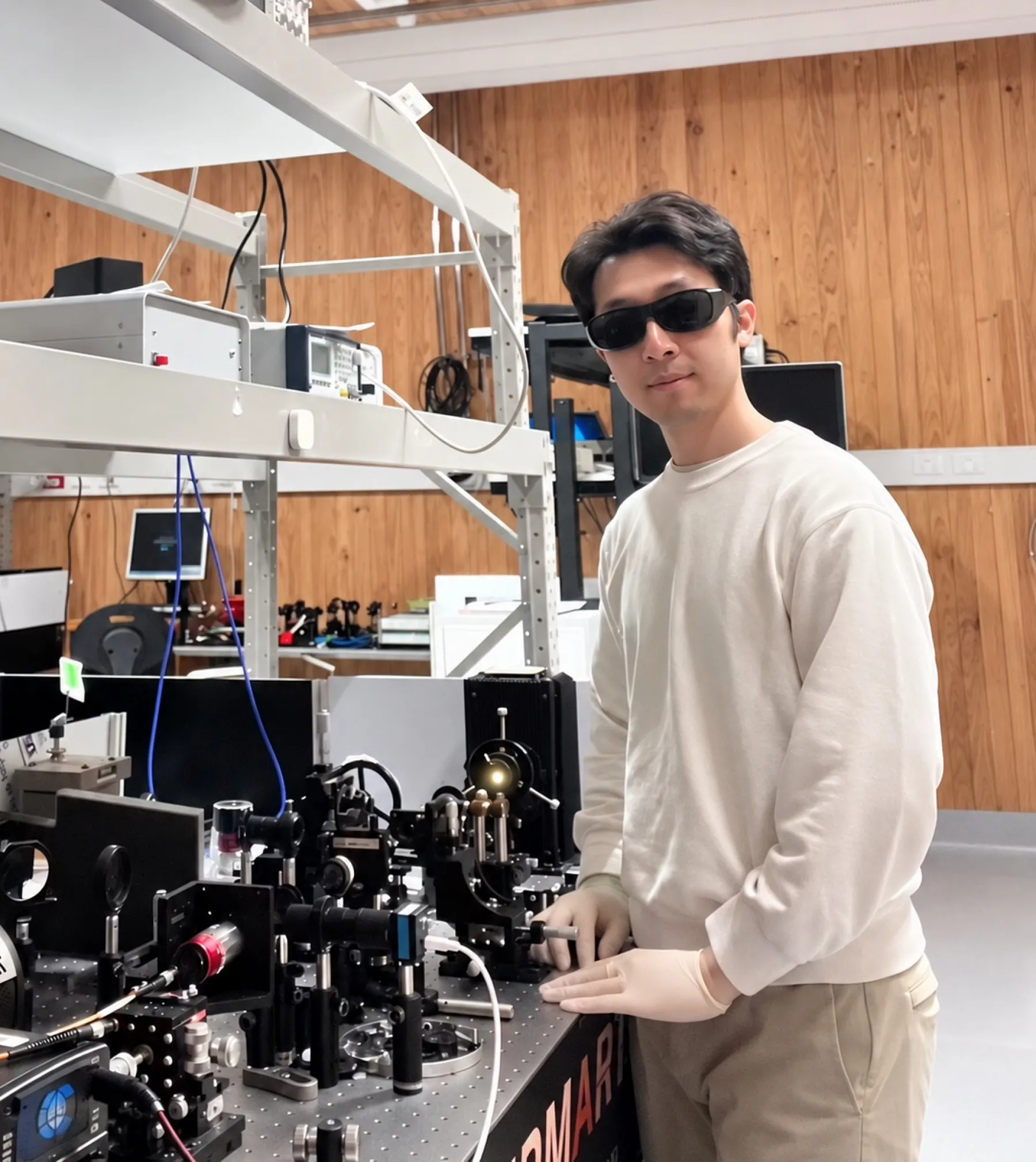 Photonics2 days agoResearchers use light to reprogram a photonic device
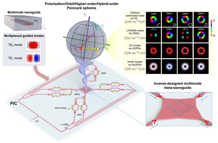 Photonics2 days agoFully tunable on-chip meta-generator mapping multidimensional Poincaré spheres
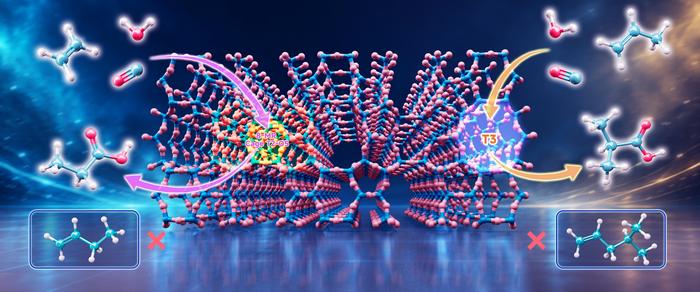 Chemistry2 days agoZeolite pore architecture unlocks new olefin carbonylation reactions
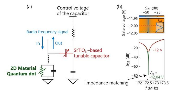 Quantum Tech3 days agoNew high-frequency method boosts 2D material readout for next-gen quantum computersNO IMAGEPhysics3 days agoA new light on one of modern physics’ greatest mysteries
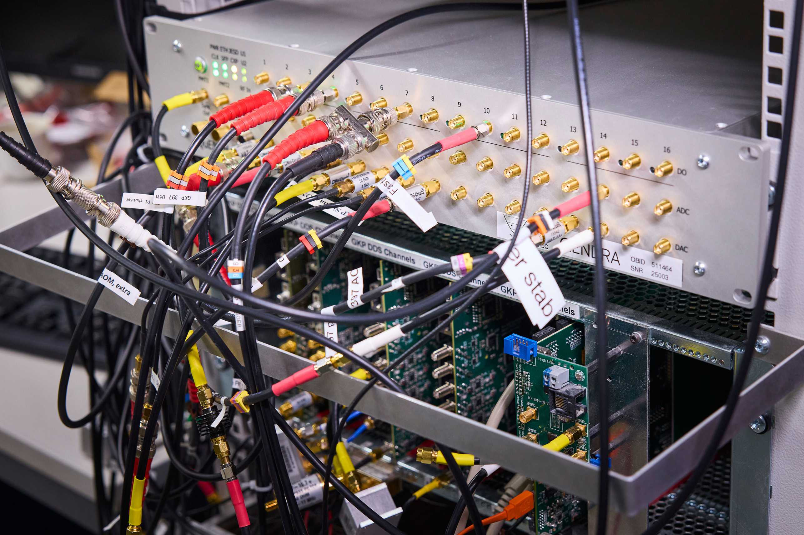 Quantum Tech3 days agoSpin-off developing “conductors” for quantum computers
 Physics3 days agoExperiment reveals quantum tug-of-war limiting higher-temperature superconductivity
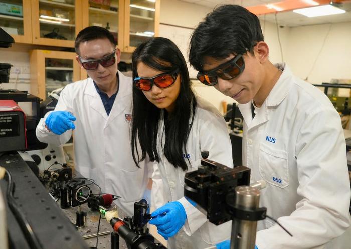 Chemistry3 days agoNUS CDE researchers map individual reactions to guide better catalyst design
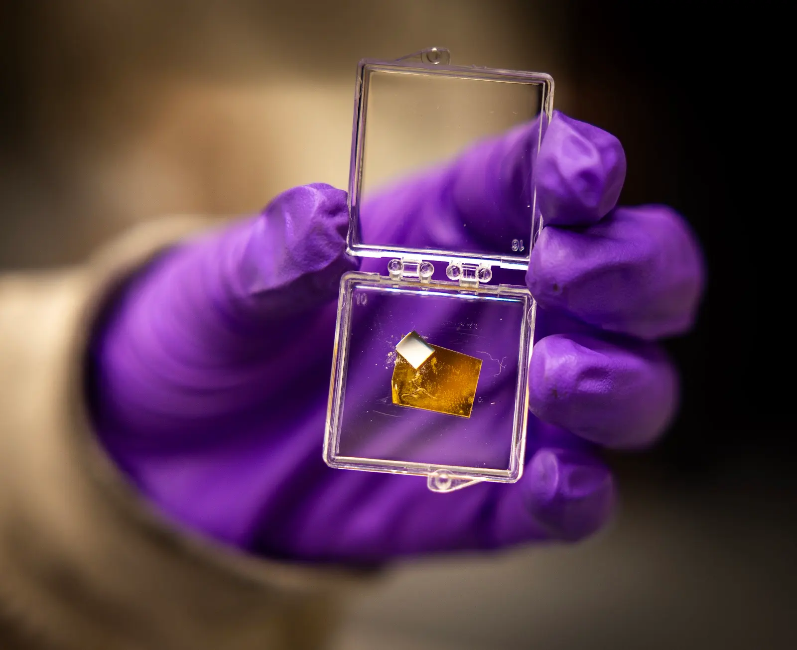 Computing3 days agoBeyond transistor limits: Hybrid magnetic-sound waves could boost computing speed and efficiency
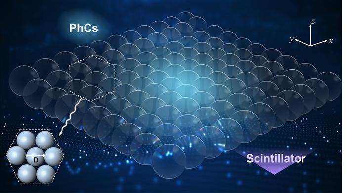 Photonics4 days agoNew photonic crystal scintillator paradigm boosts low-cost X-ray imaging sensitivity
 Order · CAD 1.64M2 days agoTekna receives titanium powder orders worth CAD 1.64 million from medical distributorABQuantum Tech2 days agoAlice & Bob Files Phase 1 Results in France's PROQCIMA Quantum ProgramCQSeed · €2.78M2 days agoCoherence Quantum Raises €2.78 Million in Seed RoundKTPartnership3 days agoKeysight, Glasgow University, NPL and MPI co-developing broadband characterization of sub-THz devices
 Quantum Tech3 days agoQuantinuum Reports 10x Reduction in Logical Error Rate on Helios
 New product3 days agoNanomate by Phi4tech certifies reduced graphene oxide rGO+ at CSIC Carbon Institute
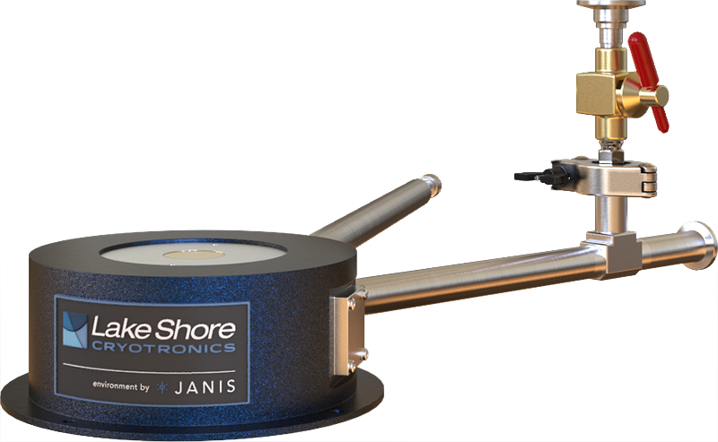 New product3 days agoLake Shore Cryotronics Highlights Cryostat Range for Spectroscopy ApplicationsHSSemiconductor3 days agoHORIBA STEC KOREA to mass produce D500 mass flow controllers from June 2021