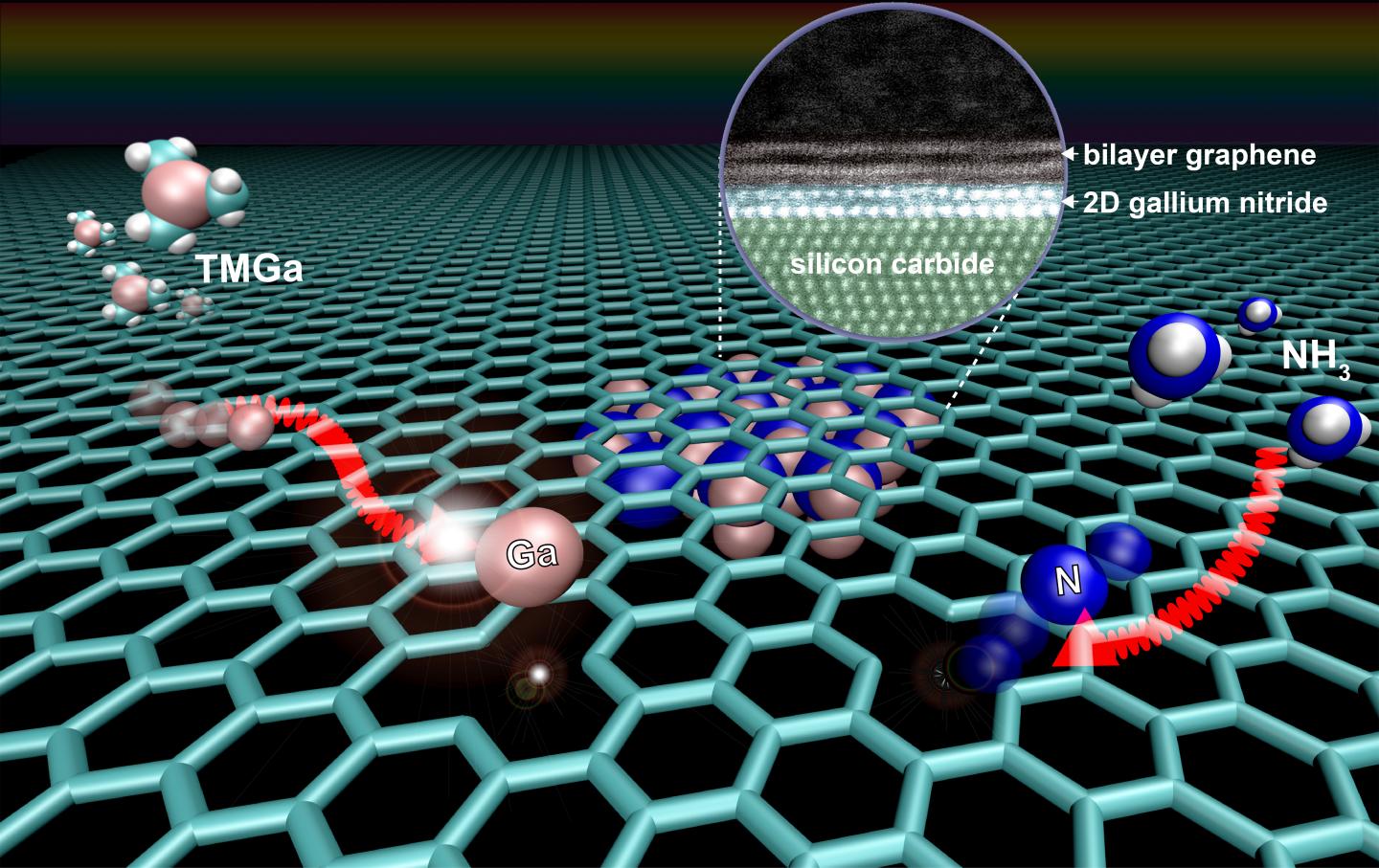
A newly discovered method for making two-dimensional materials could lead to new and extraordinary properties, particularly in a class of materials called nitrides, say the Penn State materials scientists who discovered the process. This first-ever growth of two-dimensional gallium nitride using graphene encapsulation could lead to applications in deep ultraviolet lasers, next-generation electronics and sensors.
"These experimental results open up new avenues of research in 2D materials," says Joshua Robinson, associate professor of materials science and engineering. "This work focuses on making 2D gallium nitride, which has never been done before."
Gallium nitride in its three-dimensional form is known to be a wide-bandgap semiconductor. Wide-bandgap semiconductors are important for high frequency, high power applications.
When grown in its two-dimensional form, gallium nitride transforms from a wide-bandgap material to an ultrawide-bandgap material, effectively tripling the energy spectrum it can operate in, including the whole ultraviolet, visible and infrared spectrum. This work will have a particular impact on electro-optic devices that manipulate and transmit light.
"This is a new way of thinking about synthesizing 2D materials," said Zak Al Balushi, a Ph.D. candidate coadvised by Robinson and Joan Redwing, professor of materials science and engineering and electrical engineering. Al Balushi is lead author on a paper appearing online today (Aug.29) in the journal Nature Materials titled "Two-Dimensional Gallium Nitride Realized via Graphene Encapsulation."
"We have this palette of naturally occurring 2D materials," he continued. "But to expand beyond this, we have to synthesize materials that do not exist in nature. Typically, new material systems are highly unstable. But our growth method, called Migration Enhanced Encapsulated Growth (MEEG), uses a layer of graphene to assist the growth and stabilize a robust structure of 2D gallium nitride."
The graphene is grown on a substrate of silicon carbide, which is a technologically important substrate used widely in industry for LEDs, radar and telecommunications. When heated, the silicon on the surface decomposes and leaves a carbon-rich surface that can reconstruct into graphene. The advantage of producing the graphene in this way is that the interface where the two materials meet is perfectly smooth.
Robinson believes that in the case of two-dimensional gallium nitride, the addition of a layer of graphene makes all the difference. Graphene, a one-atom-thick layer of carbon atoms, is known for its remarkable electronic properties and strength.
"It's the key," Robinson says. "If you try to grow these materials the traditional way, on silicon carbide, you normally just form islands. It doesn't grow in nice layers on the silicon carbide."
When gallium atoms are added to the mix, they migrate through the graphene and form the middle layer of a sandwich, with graphene floating on top. When nitrogen atoms are added, a chemical reaction takes place that turns the gallium and nitrogen into gallium nitride.
"The MEEG process not only produces ultra-thin sheets of gallium nitride but also changes the crystal structure of the material, which may lead to entirely new applications in electronics and optoelectronics," said Redwing.
Additional coauthors include Ke Wang, Rafael Vila, Sarah Eichfield, Yu-Chuan Lin and Shruti Subramanian of Penn State, Ram Krishna Ghosh and Suman Datta of Notre Dame, Joshua Caldwell, U.S. Naval Research Laboratory, Xiaoye Qin and Robert Wallace The University of Texas at Dallas and Dennis Paul, Physical Electronics USA.
Two-dimensional gallium nitride realized via graphene encapsulation
Zakaria Y. Al Balushi, Ke Wang, Ram Krishna Ghosh, Rafael A. Vilá, Sarah M. Eichfeld, Joshua D. Caldwell, Xiaoye Qin,Yu-Chuan Lin, Paul A. DeSario, Greg Stone, Shruti Subramanian, Dennis F. Paul, Robert M. Wallace, Suman Datta, Joan M. Redwing & Joshua A. Robinson
Nature Materials (2016) doi:10.1038/nmat4742
Penn State
#Graphene #Semiconductors #2DMaterials #MaterialScience #Nanoengineering

Waste polyamide-derived CQDs show continuous photoluminescence tuning from 308 to 552 nm through sequential defect-state engineering, with optical transition energies decreasing from 4.32 to 2.50 eV. @Christian Ebere Enyoh from Saitama University Carbon quantum dots (CQDs) are fluorescent carbon nanomaterials with potential applications in sensing, optoelectronics, displays, anti-counterfeiting, and environmental technologies. Their optical properties can be adjusted by modifying the carbon...

The researchers used circularly polarized light at normal incidence and found that helicity-dependent photocurrents appeared perpendicular to the crystal’s polarization but vanished when measured parallel to it, supporting a bulk origin of CPGE. @Institute of Science Tokyo The circular photogalvanic effect (CPGE), a phenomenon that generates helicity-dependent photocurrents in noncentrosymmetric materials, can originate purely from a crystal's internal structure without contribution from the...

Summary of gold nanoparticle growth programming in liposome based on localization of biomineralization peptide The position of biomineralization peptides within liposomes can influence how gold nanoparticles grow, reports a research team from Institute of Science Tokyo. Peptides localized at the membrane interface promote branched structures, while those confined to the liposome interior favor spherical nanoparticles. The findings offer a new strategy for controlling nanoscale reaction...