The brilliant blue of the Hope Diamond is caused by small impurities in its crystal structure. Similar diamond impurities are also giving hope to scientists looking to create materials that can be used for quantum computing and quantum sensing.
In new research from the U.S. Department of Energy’s (DOE) Argonne National Laboratory, researchers have created extremely thin membranes of pure diamond. In a few locations in the crystal structure of the membrane, however, the team substituted carbon atoms with other atoms, notably nitrogen. These defects connect to neighboring atomic vacancies — regions where an atom is missing — creating unusual quantum systems known as “color centers.” Such color centers are sites for storing and processing quantum information.
This work was supported primarily by DOE’s Office of Basic Energy Sciences, Materials Sciences and Engineering division, with support from Q-NEXT, a DOE National Quantum Information Science Research Center led by Argonne.
Equipped with a way to cheaply and easily create diamond membranes that have robust color centers, scientists at Argonne hope to build a kind of assembly line for generating large numbers of these membranes for quantum experiments around the world.
The ability to grow the membranes could be the ticket to enhancing collaboration between different laboratories devoted to quantum information science, said University of Chicago graduate student Xinghan Guo, lead author of the study.
“Essentially, we hope this will eventually give us the ability to become a one-stop shop for quantum sensing materials,” Guo said.
“The defects in the diamond are interesting to us because they can be exploited for quantum application,” said Nazar Delegan, scientist in Argonne’s Materials Science division and the Pritzker School of Molecular Engineering at the University of Chicago and a collaborator with Q-NEXT. “Making these membranes allows us to integrate these defects with other systems and enables new experimental configurations.”
Diamond is mechanically hard, chemically stable and generally expensive — in other words, it is kind of a scientific nightmare, notoriously difficult to fabricate and integrate. At the same time, diamond’s particular structure makes it a great host for color centers that can store quantum information for a long time, Guo said.
“Conventional diamond as a substrate is super hard to work with,” he said. “Our membranes are thinner and more accessible for a wide range of experiments.”
The new diamond material fashioned by the researchers offers greater crystal and surface quality, enabling greater control over the coherence of the color centers.
“You can peel the membrane off and put it on a wide range of substrates, even put it on a silicon wafer. It’s a cheap, flexible and easy way of working with color centers without having to work directly with conventional diamond,” Guo said.
“Because we’re able to control and maintain the quantum properties in individual defects within these very thin materials, it makes this platform promising as basis for a quantum technologies,” Delegan said.
Reference
Tunable and Transferable Diamond Membranes for Integrated Quantum Technologies
Xinghan Guo, Nazar Delegan, Jonathan C. Karsch, Zixi Li, Tianle Liu, Robert Shreiner, Amy Butcher, David D. Awschalom, F. Joseph Heremans, and Alexander A. High
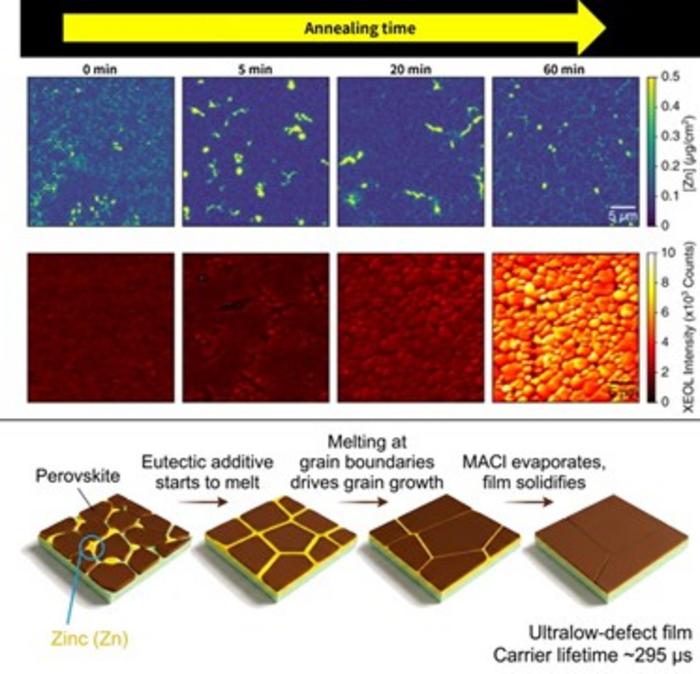
A eutectic mixture of methylammonium chloride and a zinc halide melts at about 100 degrees Celsius, forming a transient liquid layer at perovskite grain boundaries that lets crystals merge into larger, cleaner grains. The resulting films reached a carrier lifetime of roughly 295 microseconds and a surface recombination velocity of 0.3 cm/s, the lowest reported for lead halide perovskites.
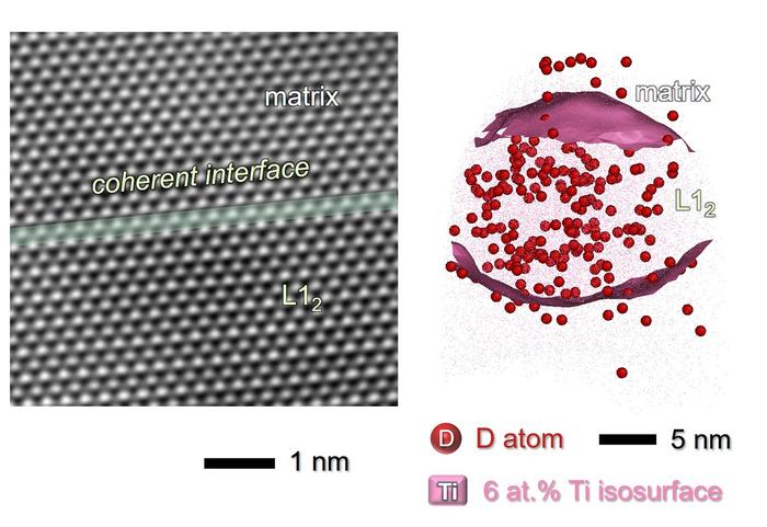
Researchers at the University of Sydney have directly observed hydrogen dissolved in the interstitial spaces between metal atoms in alloys, a world first. Using cryogenic atom probe tomography with deuterium tracers, electron microscopy and theoretical calculations, the team showed hydrogen occupies sites between atoms rather than only collecting at defects, and that local atomic arrangement and chemistry dictate where it prefers to reside.
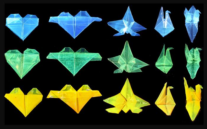
Researchers have developed carbon dots whose fluorescence shifts across the visible spectrum, from blue to red, depending on concentration, liquid environment and acidity. By tuning the particles' surfaces, the team produced versions that change color reversibly as pH shifts, then incorporated them into polymer powders, molded shapes and flexible films.
This week in nanotech
$10.2M raised
1 funding round · 13 deals tracked
New products
 Nion-compatible In Situ STEM Holders for Electrical BiasingHummingbird Scientific Featured
 Ti-WCMBN Nanomaterialia Featured
 Hold Down & Release Mechanisms (HDRM) REACT – 5KN, 15KN and 35KN space qualified resettable mechanismsARQUIMEA
Market insights
Last 30 days: Quantum Technologies was the busiest vertical: 52 of 174 events (30%).
Money raised per month
Behind the deal
Who led Sandia National Laboratories’s $3.4M Grant?
See the investors with Insights Pro →