Broad spectrum
- Apr 13, 2020
- 3 min read
Updated: Apr 17, 2020

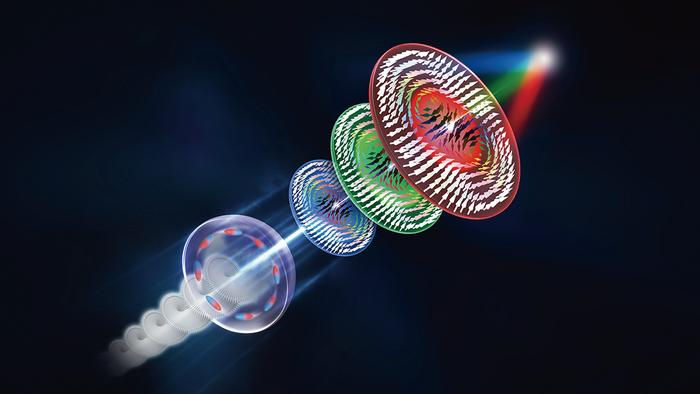
Digital cameras as well as many other electronic devices need light-sensitive sensors. In order to cater for the increasing demand for optoelectronic components of this kind, industry is searching for new semiconductor materials. They are not only supposed to cover a broad range of wavelengths but should also be inexpensive. A hybrid material, developed in Dresden, fulfils both these requirements. Himani Arora, a physics PhD student at Helmholtz-Zentrum Dresden-Rossendorf (HZDR), demonstrated that this metal-organic framework can be used as a broadband photodetector. As it does not contain any cost-intensive raw materials, it can be produced inexpensively in bulk. In the last twenty years, metal-organic frameworks (MOFs) have become a coveted material system. So far, these highly porous substances, up to 90 percent of which are composed of empty space, have largely been used to store gases, for catalysis or to slowly release drugs in the human body. "The metal-organic framework compound developed at TU Dresden comprises an organic material integrated with iron ions," explains Dr. Artur Erbe, head of the "Transport in Nanostructures" group at HZDR's Institute of Ion Beam Physics and Materials Research. "The special thing about it is that the framework forms superimposed layers with semiconducting properties, which makes it potentially interesting for optoelectronic applications." The group had the idea of using the new semiconducting two-dimensional MOF as a photodetector. In order to pursue it further, Himani Arora investigated the semiconductor's electronic properties. She explored, among others, to what extent the light sensitivity was dependent on temperature and wavelength - and came to a promising conclusion: From 400 to 1,575 nanometers, the semiconductor could detect a broad range of light wavelengths. The spectrum of radiation thus goes from ultraviolet to near infrared. "This is the first time we have proved such a broadband photodetection for a photodetector completely based on MOF layers," the doctoral candidate notes. "These are ideal properties for using the material as an active element in optoelectronic components." Small bandgap makes for efficiency The spectrum of wavelengths a semiconducting material can cover and transform into electrical signals essentially depends on the so-called bandgap. Experts use this term to describe the energetic distance between the valence band and the conduction band of a solid state material. In typical semiconductors, the valence band is completely full, so the electrons cannot move around. The conduction band, on the other hand, is largely empty, so the electrons can move around freely and influence the current flow. While the bandgap in insulators is so big that the electrons cannot jump from the valance band to the conduction band, metal conductors have no such gaps. A semiconductor's bandgap is just big enough to raise the electrons to the higher energy level of the conduction band by using the light waves. The smaller the bandgap, the lesser the energy required to excite an electron. "As the bandgap in the material we explored is very small, only very little light energy is required to induce the electricity," Himani Arora explains. "This is the reason for the large range of the detectable spectrum." By cooling the detector down to lower temperatures, the performance can be improved yet further because the thermal excitation of the electrons is suppressed. Other improvements include optimizing the component configuration, producing more reliable contacts and developing the material further. The results suggest that the MOF-based photodetectors will have a bright future. Thanks to their electronic properties and inexpensive manufacturing, MOF layers are promising candidates for a raft of optoelectronic applications. "The next step is to scale the layer thickness," says Artur Erbe, looking forward. "In the study, 1.7 micrometer MOF films were used to build the photodetector. To integrate them into components, they need to be significantly thinner." If possible, the aim is to reduce the superimposed layers to 70 nanometers, that is, 25 times smaller than their size. Down to this layer thickness the material should exhibit comparable properties. If the group can prove that the functionality remains the same in these significantly thinner layers, they can then embark on developing it to the production stage. Demonstration of a broadband photodetector based on a two-dimensional metal-organic framework H. Arora, R. Dong, T. Venanzi, J. Zscharschuch, H. Schneider, M. Helm, X. Feng, E. Cánovas, A. Erbe Advanced Materials (2020) DOI: 10.1002/adma.201907063 Contact information: Artur Erbe | Himani Arora Institute of Ion Beam Physics and Materials Research at HZDR a.erbe@hzdr.de | h.arora@hzdr.de Phone: +49 351 260-2366 Helmholtz-Zentrum Dresden-Rossendorf (HZDR)
Learn more about the Nanotechnology World Association (NWA):


Trong thời gian trải nghiệm trang chủ gemwin, mình thấy nền tảng chú trọng khá nhiều vào khả năng điều hướng thông qua hệ thống menu được tổ chức khoa học. Các khu vực như casino trực tuyến, game bài đổi thưởng, nổ hũ và bắn cá được đặt tại vị trí dễ quan sát giúp việc lựa chọn nội dung trở nên đơn giản hơn. Mình nhận thấy điều này hỗ trợ người dùng tiết kiệm đáng kể thời gian tìm kiếm. Khi thử nghiệm giữa casino và nổ hũ, thao tác chuyển trang diễn ra khá nhanh, giao diện phản hồi ổn định và trải nghiệm tổng thể mang lại cảm giác mượt mà
Khi tìm hiểu về uy88.com , mình chú ý đến khu vực Roulette và cách hệ thống sắp xếp các nội dung liên quan. Bên cạnh đó, ứng dụng di động cũng là phần mình quan tâm vì hỗ trợ truy cập khá linh hoạt. Việc kết hợp giữa nội dung giải trí và khả năng sử dụng trên nhiều thiết bị giúp trải nghiệm có cảm giác liền mạch hơn. Theo mình, đây là hướng phát triển phù hợp với xu hướng hiện nay.
When I look at a platform, I usually start by observing how the interface is arranged, and tài xỉu sunwin gave me a fairly comfortable first impression. I spent some time around fishing games before moving to the account section, and the transitions between categories still felt steady. The overall design seemed to avoid unnecessary clutter, which helped make longer browsing sessions feel lighter.
After using Sun Win across different days, I started noticing how smaller details could shape the overall experience. On some evenings, I explored lottery-style sections before opening account tools, while the platform still felt relatively easy to follow. I usually appreciate layouts that stay simple even after longer sessions.
Mình hay tò mò xem một nền tảng phát triển khu game bài như thế nào và nhà cái cm88 cũng vậy. Có hôm mình mở Phỏm, sau đó chuyển sang Mậu binh rồi khám phá thêm Poker để nhìn cách các phòng chơi được xây dựng. Bên cạnh đó mình cũng khá chú ý việc hệ thống hợp tác với nhiều nhà phát hành quốc tế nên nội dung khá đa dạng. Theo mình, đây là điểm khá thú vị.