top of page
NEWSROOM


2D crystals conforming to 3D curves create strain for engineering quantum devices
A team led by scientists at the Department of Energy’s Oak Ridge National Laboratory explored how atomically thin two-dimensional (2D)...
Jun 3, 20194 min read


Measurement of semiconductor material quality is now 100,000 times more sensitive
The enhanced power of the new measuring technique to characterize materials at scales much smaller than any current technologies will...
Apr 11, 20193 min read
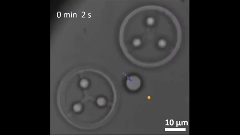
Research paves the way for next generation of optical tweezers
Scientists have developed a pioneering new technique that could pave the way for the next generation of optical tweezers. A team of...
Mar 21, 20192 min read


Physicists proposed fast method for printing nanolasers from perovskites
An international research team has developed a new method of synthesizing miniature light sources. It is based on a special laser which...
Mar 18, 20192 min read


When semiconductors stick together, materials go quantum
A team of researchers led by the Department of Energy's Lawrence Berkeley National Laboratory (Berkeley Lab) has developed a simple...
Mar 7, 20193 min read


New blueprint for understanding, predicting and optimizing complex nanoparticles
Northwestern University researchers have developed a blueprint for understanding and predicting the properties and behavior of complex...
Feb 28, 20192 min read
bottom of page