Vienna University of Technology (TU Wien)
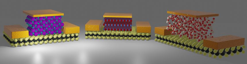
Ever smaller and ever more compact - this is the direction in which computer chips are developing, driven by industry. This is why so-called 2D materials are considered to be the great hope: they are as thin as a material can possibly be, in extreme cases they consist of only one single layer of atoms. This makes it possible to produce novel electronic components with tiny dimensions, high speed and optimal efficiency.
However, there is one problem: electronic components always consist of more than one material. 2D materials can only be used effectively if they can be combined with suitable material systems - such as special insulating crystals. If this is not considered, the advantage that 2D materials are supposed to offer is nullified. A team from the Faculty of Electrical Engineering at the TU Wien (Vienna) is now presenting these findings in the journal Nature Communications.
Reaching the end of the line on the atomic scale
"The semiconductor industry today uses silicon and silicon oxide," says Prof. Tibor Grasser from the Institute of Microelectronics at the TU Wien. "These are materials with very good electronic properties. For a long time, ever thinner layers of these materials were used to miniaturize electronic components. This worked well for a long time - but at some point we reach a natural limit".
When the silicon layer is only a few nanometers thick, so that it only consists of a few atomic layers, then the electronic properties of the material deteriorate very significantly. "The surface of a material behaves differently from the bulk of the material - and if the entire object is practically only made up of surfaces and no longer has a bulk at all, it can have completely different material properties."
Therefore, one has to switch to other materials in order to create ultra-thin electronic components. And this is where the so-called 2D materials come into play: they combine excellent electronic properties with minimal thickness.
Thin layers need thin insulators
"As it turns out, however, these 2D materials are only the first half of the story," says Tibor Grasser. "The materials have to be placed on the appropriate substrate, and an insulator layer is also needed on top of it - and this insulator also hast to be extremely thin and of extremely good quality, otherwise you have gained nothing from the 2D materials. It's like driving a Ferrari on muddy ground and wondering why you don't set a speed record."
A team at the TU Wien around Tibor Grasser and Yury Illarionov has therefore analysed how to solve this problem. "Silicon dioxide, which is normally used in industry as an insulator, is not suitable in this case," says Tibor Grasser. "It has a very disordered surface and many free, unsaturated bonds that interfere with the electronic properties in the 2D material."
It is better to look for a well-ordered structure: The team has already achieved excellent results with special crystals containing fluorine atoms. A transistor prototype with a calcium fluoride insulator has already provided convincing data, and other materials are still being analysed.
"New 2D materials are currently being discovered. That's nice, but with our results we want to show that this alone is not enough," says Tibor Grasser. "These new electrically conductive 2D materials must also be combined with new types of insulators. Only then can we really succeed in producing a new generation of efficient and powerful electronic components in miniature format".
Insulators for 2D nanoelectronics: the gap to bridge
Yury Yu. Illarionov, Theresia Knobloch, Markus Jech, Mario Lanza, Deji Akinwande, Mikhail I. Vexler, Thomas Mueller, Max C. Lemme, Gianluca Fiori, Frank Schwierz & Tibor Grasser
Nature Communications volume 11, Article number: 3385 (2020)
DOI: 10.1038/s41467-020-16640-8
Contact information:
Professor, Institute for Microelectronics, TU Wien
tibor.grasser@tuwien.ac.at
Phone: +43-1-58801-36000

Waste polyamide-derived CQDs show continuous photoluminescence tuning from 308 to 552 nm through sequential defect-state engineering, with optical transition energies decreasing from 4.32 to 2.50 eV. @Christian Ebere Enyoh from Saitama University Carbon quantum dots (CQDs) are fluorescent carbon nanomaterials with potential applications in sensing, optoelectronics, displays, anti-counterfeiting, and environmental technologies. Their optical properties can be adjusted by modifying the carbon...

The researchers used circularly polarized light at normal incidence and found that helicity-dependent photocurrents appeared perpendicular to the crystal’s polarization but vanished when measured parallel to it, supporting a bulk origin of CPGE. @Institute of Science Tokyo The circular photogalvanic effect (CPGE), a phenomenon that generates helicity-dependent photocurrents in noncentrosymmetric materials, can originate purely from a crystal's internal structure without contribution from the...

Summary of gold nanoparticle growth programming in liposome based on localization of biomineralization peptide The position of biomineralization peptides within liposomes can influence how gold nanoparticles grow, reports a research team from Institute of Science Tokyo. Peptides localized at the membrane interface promote branched structures, while those confined to the liposome interior favor spherical nanoparticles. The findings offer a new strategy for controlling nanoscale reaction...
