Scientists at the University of Warwick and the National Research Council of Canada have achieved and measured the highest “hole mobility” ever recorded in a silicon-compatible material.
Most modern semiconductors are fabricated of or on Silicon (Si), but as devices get smaller and denser, they dissipate more power and as a result, are reaching their physical limits. Germanium (Ge)— once used in the first transistors of the 1950s — is now making a comeback as researchers find new ways to harness its superior properties while keeping the benefits of silicon’s established manufacturing technologies.
In a new study, published in Materials Today, a team led by Warwick’s Dr Maksym Myronov achieved a major step towards the next generation of electronics — creating a material using a nanometre-thin, compressively strained germanium epilayer on silicon, that allows electrical charge to move faster than ever before in a material compatible with modern chipmaking.
Maksym Myronov, Associate Professor and leader of the Semiconductors Research Group, Department of Physics, University of Warwick says “Traditional high-mobility semiconductors such as gallium arsenide (GaAs) are very expensive and impossible to integrate with mainstream silicon manufacturing. Our new compressively strained germanium-on-silicon (cs-GoS) quantum material combines world-leading mobility with industrial scalability — a key step toward practical quantum and classical large-scale integrated circuits.”
The breakthrough was achieved by carefully engineering a thin germanium layer on top of a silicon wafer. By applying just the right amount of strain to the germanium layer, they created an ultra-clean crystal structure that allows electrical charge to flow almost without resistance.
When evaluated, the material demonstrated a record hole mobility of 7.15 million cm² per volt-second (compared to *** in industrial silicon), meaning charge can move through it far more easily than in silicon. This could enable future chips to run faster and dissipate less energy.
Dr Sergei Studenikin, Principal Research Officer, National Research Council of Canada adds: “This sets a new benchmark for charge transport in group-IV semiconductors – the materials at the heart of the global electronics industry. It opens the door to faster, more energy-efficient electronics and quantum devices that are fully compatible with existing silicon technology.”
The research establishes a new pathway for ultra-fast, low-power electronics, with potential applications spanning quantum information processing, spin qubits, cryogenic controllers for quantum processors, AI, and data-centre hardware with reduced energy and cooling demands.
This advance also marks a major milestone for Warwick’s Semiconductors Research Group, reinforcing the UK’s leadership in semiconductor materials science.
Reference
Hole mobility in compressively strained germanium on silicon exceeds 7 × 10⁶ cm²V⁻¹s⁻¹
Maksym Myronov, Alex Bogan, Sergei Studenikin
https://www.sciencedirect.com/science/article/pii/S1369702125004237
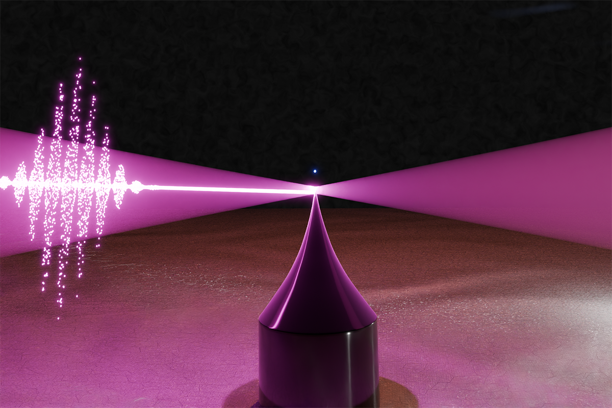
For a long time, the two areas of strong-field physics and quantum optics were considered independent areas of physics research without any significant overlaps. Whilst strong-field physics focuses on the behavior of material, such as atomic gases, in intense light fields, quantum optics focuses on researching special quantum properties of light that cannot be described within the framework of classical physics. Strong-field physics requires intense laser rays, in other words rays with innume...
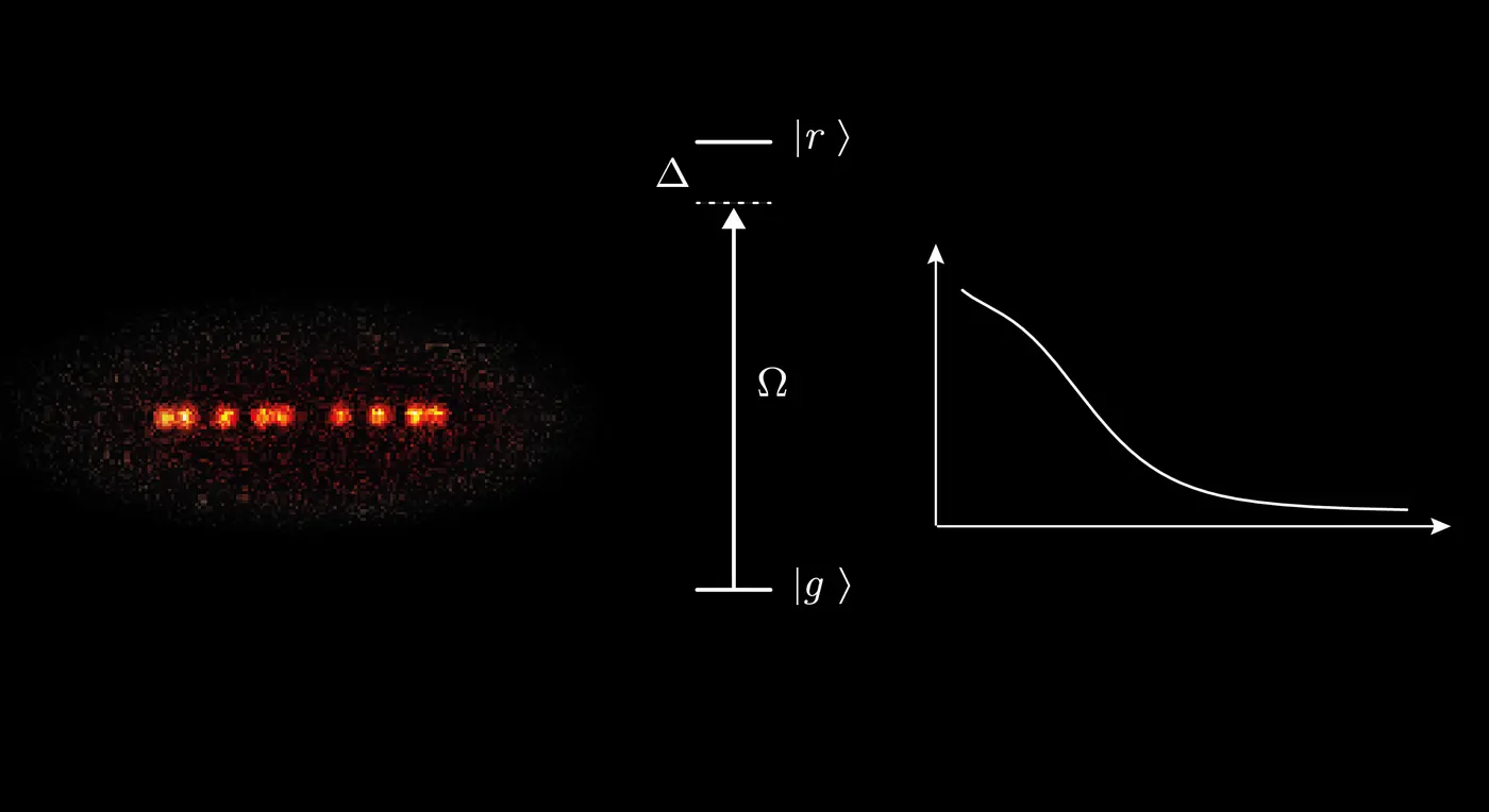
A research team from the Max Planck Institute of Quantum Optics succeeded in realising tuneable long-range interactions between atoms. In their study, published in Science, the scientists were able to increase the system’s lifetime by more than a factor of 100 compared to previous experiments. This allows to study the effect of long-range interactions on a microscopic level in tunnel-coupled quantum systems. Notably, the team experimentally observed an unusual binding mechanism of two atoms a...
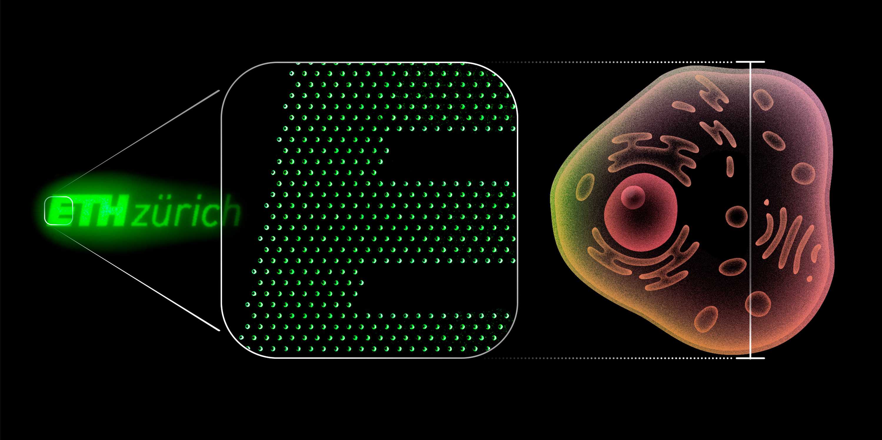
On the one hand, pixels ranging in size from 100 to 200 nanometres form the foundation for ultra-high-resolution screens that could display razor-sharp images in glasses worn close to the eye, for example. In order to illustrate this, Shih's team of researchers displayed the ETH Zurich logo. This ETH logo consists of 2,800 nano-OLEDs and is similar in size to a human cell, with each of its pixels measuring around 200 nanometres (0.2 micrometres). The smallest pixels developed so far by the ET...
This week in nanotech
$741.8M raised
4 funding rounds · 24 deals tracked
New products
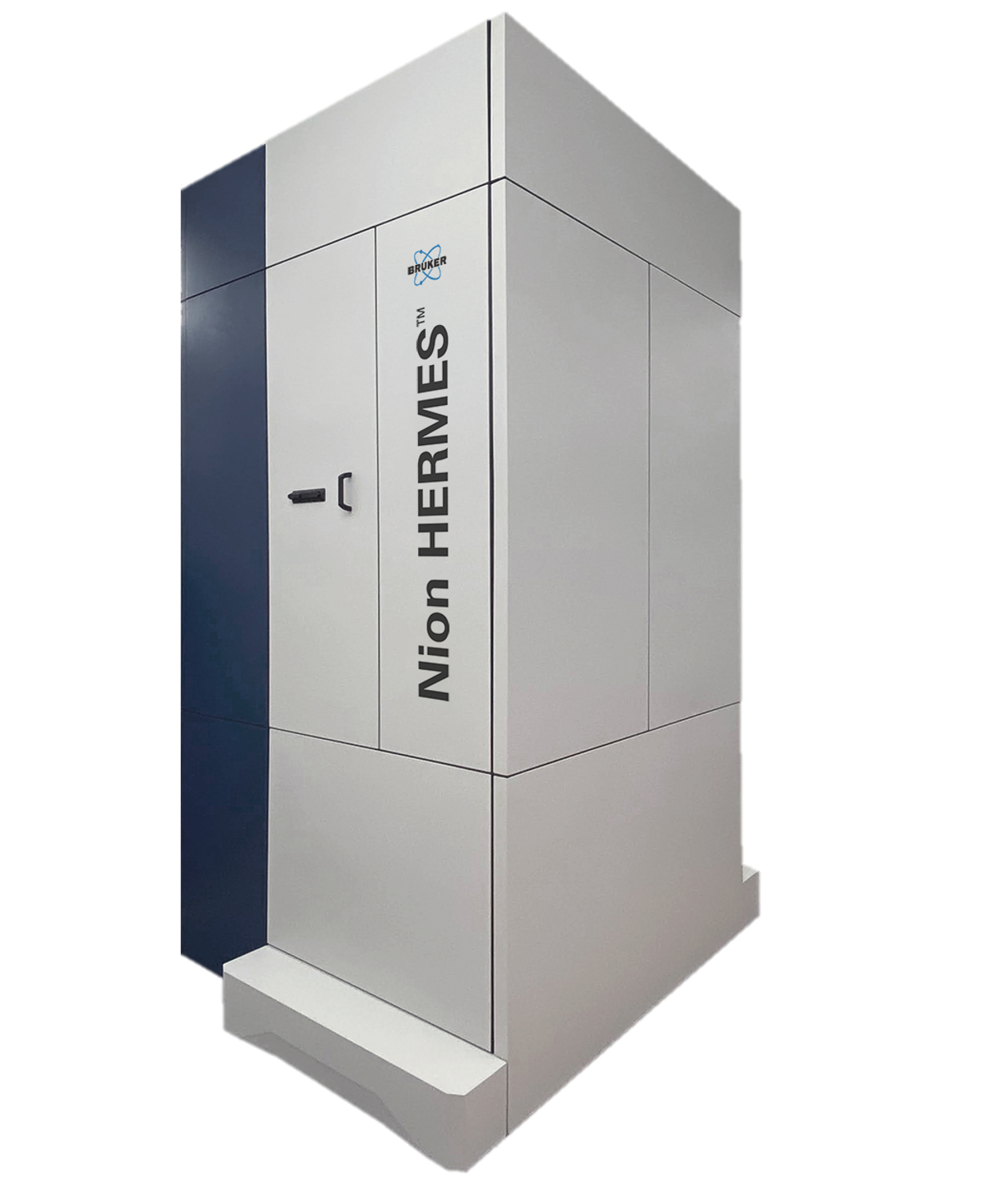 Nion-compatible In Situ STEM Holders for Electrical BiasingHummingbird Scientific Featured
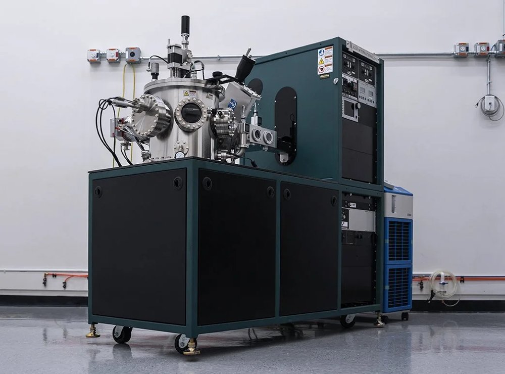 Orion Sputtering Deposition SystemsAJA International Featured
 GiiiGii
Market insights
Last 30 days: Quantum Technologies drew the most money: $3.17B.
Money raised per month
Behind the deal
Who invested in Photon Bridge’s $11.2M Series A?
See the investors with Insights Pro →